Display device
a display device and display technology, applied in the field of electronic displays, can solve the problems of large change in the electric potential of the power supply line due to the resistance of the wiring, the potential drop of the connection wiring portion, and the change in the electric potential of the power supply lin
- Summary
- Abstract
- Description
- Claims
- Application Information
AI Technical Summary
Problems solved by technology
Method used
Image

Examples
embodiment 1
[0154] (Embodiment 1)
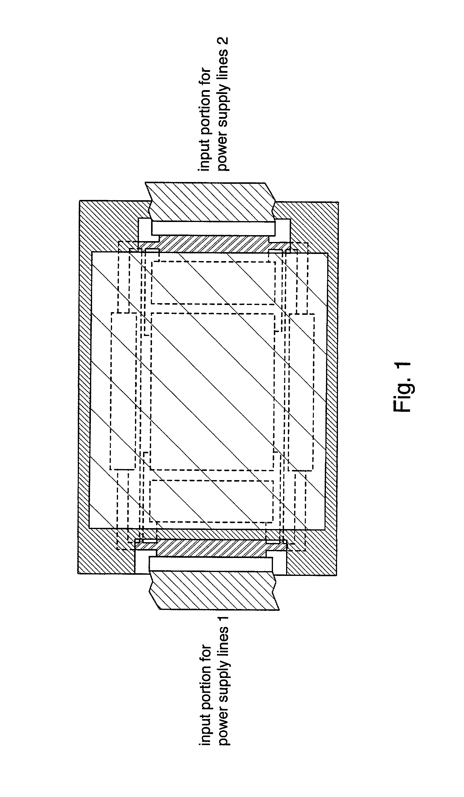
[0155] FIG. 4 illustrates an example where a small number of power supply lines are collected together in one unit and are connected to an external input terminal, which is described in Embodiment 2.
[0156] Since the potential drop becomes larger as the size of the display becomes larger, it is necessary to make the wirings as short as possible which draw out the power supply lines. According to the present invention, a small number of power supply lines are collected together in one unit, and are outputted to an adjacent external input terminal.
[0157] In the example illustrated in FIG. 4, a small number of power supply lines are collected together in one unit, and are connected to an external input terminal through a driver region. In this way, the wiring resistance is decreased.
[0158] It is desirable that about five to fifty power supply lines are collected together in one unit.
embodiment 2
[0159] (Embodiment 2)
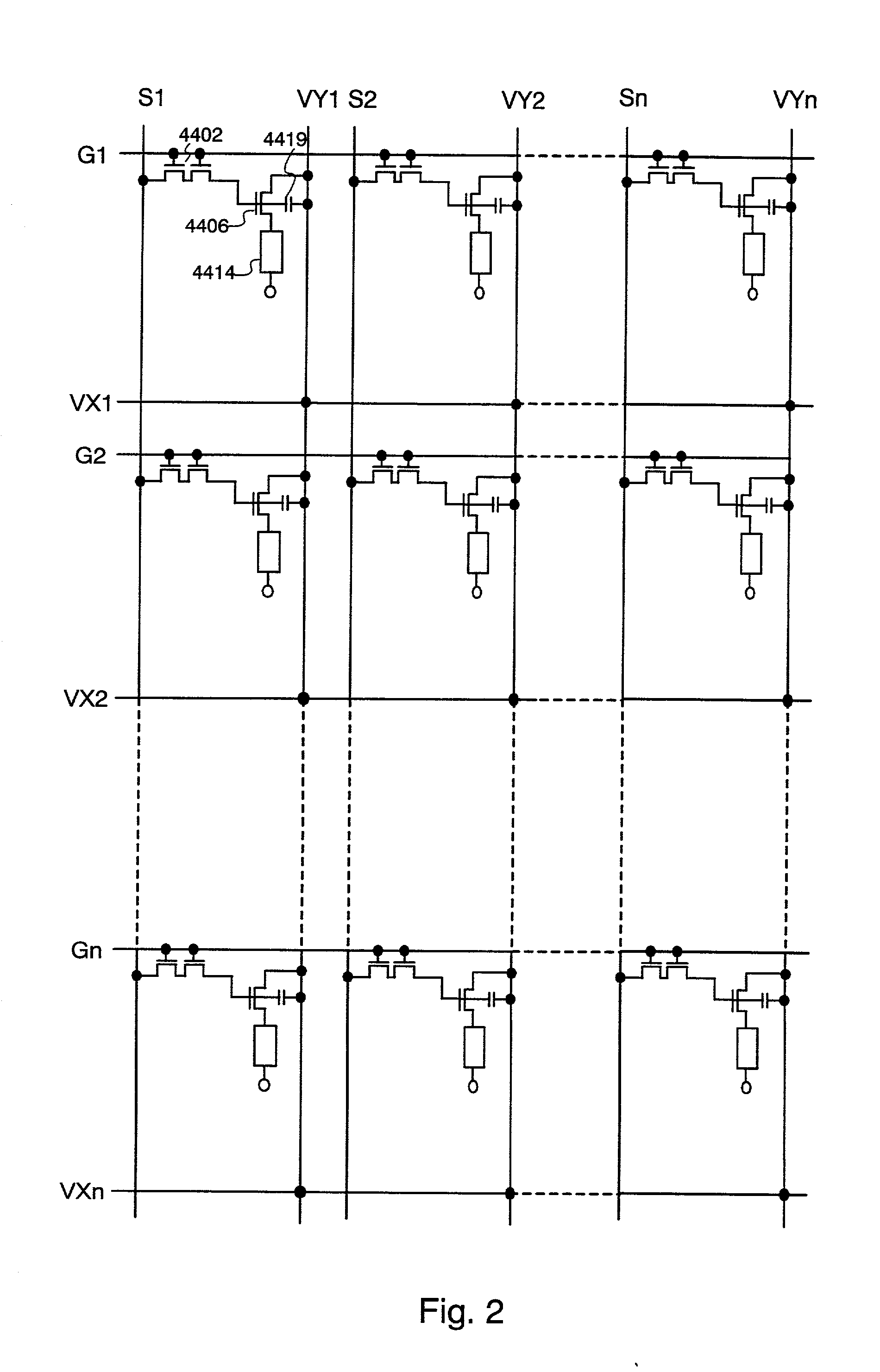
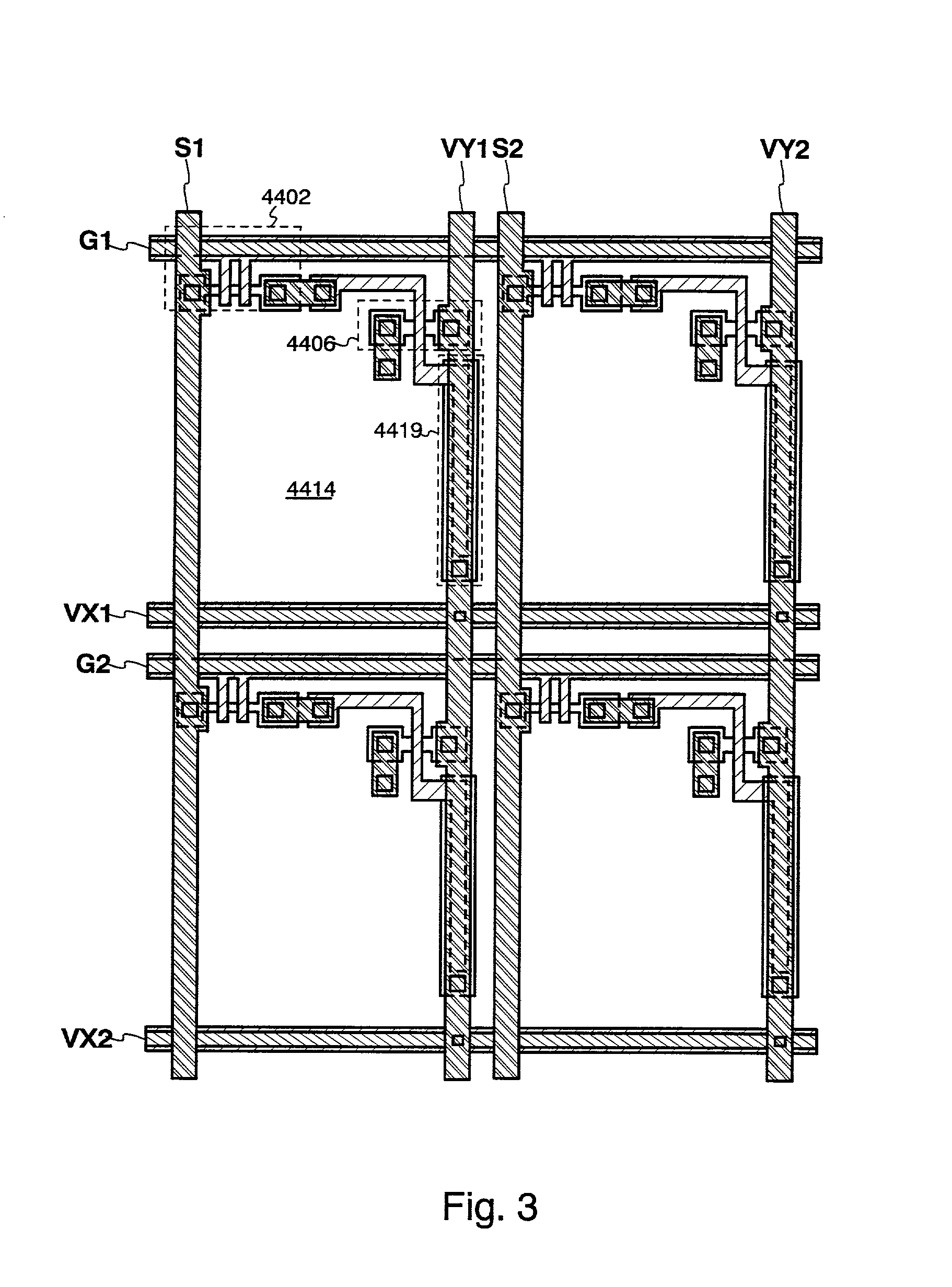
[0160] FIG. 3 is a top view of a part (four pixels) of the pixel portion of the circuit diagram illustrated in FIG. 2 as an embodiment of the present invention.
[0161] It is to be noted that like reference numerals designate like parts in FIG. 2.
[0162] Each pixel is formed of a TFT 4402 for switching, a TFT 4406 for driving, a capacitor 4419, and an EL element 4414. In this embodiment, power supply lines VX1 and VX2 are disposed in parallel with gate signal lines G1 and G2 using a wiring material similar to that of the gate signal lines G1 and G2. The power supply lines VX1 and VX2 are connected through contact holes to conventional power supply lines VY1 and VY2 in parallel with the source signal lines S1 and S2.
[0163] A structure where power supply lines in parallel with the gate signal lines are formed using a wiring layer forming the gate signal lines as the present embodiment is herein referred to as Embodiment 1 of a pixel structure according to the present...
embodiment 3
[0166] (Embodiment 3)
[0167] In the present embodiment, a case where power supply lines are shared between pixels next to each other described in Embodiment 4 is described with reference to FIGS. 10 and 42-44.
[0168] It is to be noted that, in the present embodiment, G1-G4 are gate wirings (a part of gate signal lines) of a TFT 4402 for switching, S1-S3 are source wirings (a part of source signal lines) of the TFT 4402 for switching, 4406 is a TFT for driving, 4414 is an EL element, VY1-VY2 are power supply lines in parallel with the source wirings, VX1-VX2 are power supply lines in parallel with the gate wirings, and 4419 is a storage capacitor.
[0169] FIG. 10 illustrates a case where the power supply lines VY1 and VX1 are shared between two pixels next to each other. It is characteristic that the two pixels are formed so as to be symmetrical with respect to the power supply lines VY1 and VX1. In this case, since the number of the power supply lines can be decreased, the aperture rati...
PUM
 Abstract
Description
Claims
Application Information
 - Generate Ideas
- Intellectual Property
- Life Sciences
- Materials
- Tech Scout
- Unparalleled Data Quality
- Higher Quality Content
- 60% Fewer Hallucinations
Browse by: Latest US Patents, China's latest patents, Technical Efficacy Thesaurus, Application Domain, Technology Topic, Popular Technical Reports.
© 2025 PatSnap. All rights reserved.Legal|Privacy policy|Modern Slavery Act Transparency Statement|Sitemap|About US| Contact US: help@patsnap.com