
Logic gate cell

a logic gate and cell technology, applied in the field of logic gate cells, can solve the problems of poor area utilization, cell height layout, and cell area, and achieve the effect of low power consumption and high area utilization

Inactive Publication Date: 2002-01-03
A I L
View PDF0 Cites 12 Cited by
  • Summary
  • Abstract
  • Description
  • Claims
  • Application Information

AI Technical Summary

Benefits of technology

[0008] Accordingly, an object of the present invention is to provide a high area-utilization and small-area logic gate cell which employs a layout that narrows a cell width (the horizontal length as shown in drawings) instead of lowering the cell height, to realize a low power consuming logic gate cell based on a narrow gate width transistor.
[0011] A logic gate cell having an even narrower gate width is provided by forming the first inverting logic gate output wirings of the first metal layer wirings, and by extending the second metal layer wirings of the output portion of the second inverting logic gate, over the first metal layer wirings. Specifically, since the first metal layer wirings of the output portion of the first inverting logic gate have no connection external to the cell, no problem is presented at all even if the second metal layer extends over the first inverting logic gate, and with the arrangement, the cell width is reduced to a minimum grid number required to route input and output terminals from within the cell.
[0013] In addition to the above means, a gate width of the transistor formed in the external diffusion regions and used in the second inverting logic gate is set to be wider than a gate width of the transistor formed in the internal diffusion regions and used in the first inverting logic gate, and a high drive power (with a small loading delay) and a low power consuming logic gate cell is provided.
[0015] In the logic gate cell having a circuit arrangement in which the second inverting logic gate is a NOT gate and an output of a third inverting logic gate is connected to an input of the preceding first inverting logic gate, the first and third inverting logic gates are formed using the internal diffusion regions while the second logic gate is formed using the external diffusion regions, and the above means is thus applied in the embodiment, and a small-area and low-power consuming logic gate cell is thus provided.

Problems solved by technology

The above methods present the following problems.
Secondly, as the cell height is lowered, there is no choice but to arrange a plurality of transistors horizontally side by side and connect them, to realize a high-power (wide gate width) transistor, and a horizontally elongated cell results, suffering a poor area utilization and the cell area, on the contrary, increases more than that in the high cell height layout.
These problems arise as a result of attempting lower the cell height to reduce the cell area.

Method used


Image

  • Logic gate cell
  • Logic gate cell
  • Logic gate cell

Examples


embodiments

[0175] Other embodiments of the present invention will be now explained. The following embodiments correspond to any of Claims 1 to 24.

[0176] FIGS. 28A shows a layout of a two-input AND gate AND2, and its circuit is shown in FIG. 9. The layout in FIG. 28A is different from that in FIG. 14 in that the output portions of transistors 33 and 36 are not connected in parallel, and both layouts are identical in the remaining construction. FIG. 28B shows diffusion regions and gate polysilicon wirings extracted from the layout shown in FIG. 28A. FIG. 29A shows first metal layer wirings extracted from the layout in FIG. 28A, and FIG. 29B shows second metal layer wirings extracted from the layout in FIG. 28A. The same drawing method applies in the subsequent embodiments.

[0177] FIGS. 30A and 30B and FIGS. 31A and 31B show the layout of a two-input OR gate OR2. Referring to FIG. 32B, the gate OR2 is formed by connecting a gate NOR2 and a NOT gate. FIG. 33 is a circuit diagram of the gate OR2. Th...


PUM


Abstract

To provide a small-area and low-power-consuming logic gate cell which is constructed of a circuit of two inverting logic gates connected in series in a layout of four-step diffusion regions. A first inverting logic gate is formed of a small transistor on internal two-step diffusion regions, a second inverting logic gate is formed of external two-step diffusion regions, and output wirings of the second inverting logic gate is formed of second metal layer wirings so that the second metal layer wirings extend over the first inverting logic gate.

Description

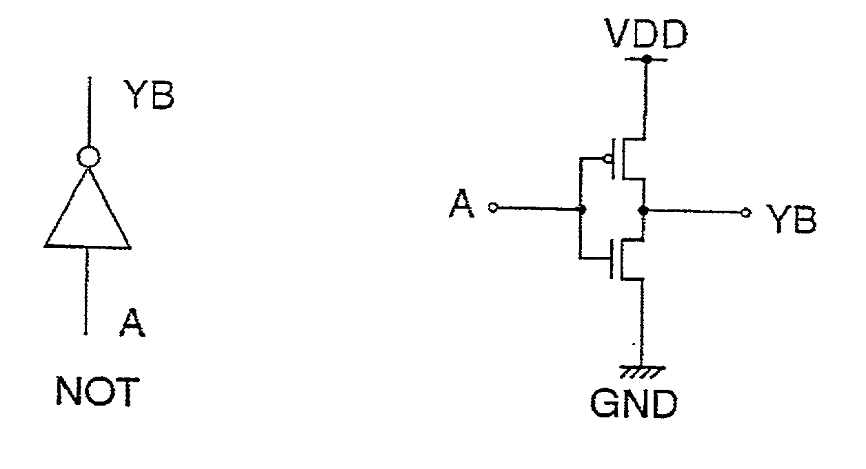
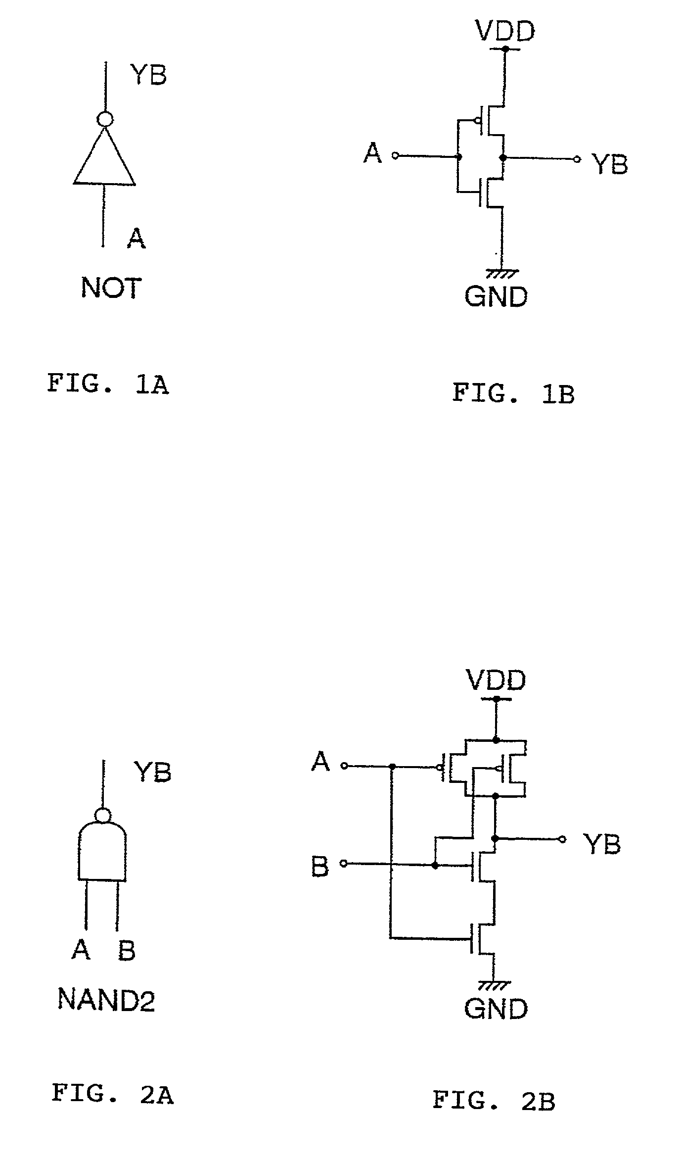
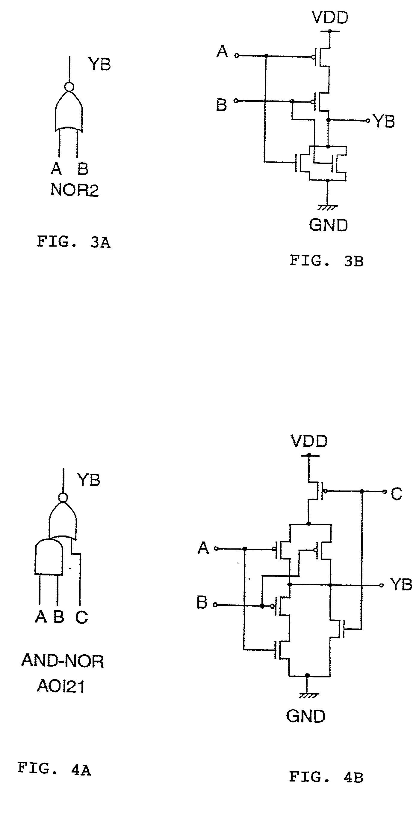
BACKGROUND OF THE INVENTION[0001] 1. Field of the Invention[0002] The present invention relates to logic gate cells used as an element in an LSI designed in a standard cell format and falls within the layout design technology of the logic gate cell manufactured in CMOS processes, and particularly to a logic gate cell featuring a small area and low power consumption.[0003] 2. Description of the Related Art[0004] A cell having a circuit arrangement of two inverting logic gates connected is frequently used for a logic gate cell that is an element when an LSI is designed using a standard cell technology. The inverting logic gates here refer to a NAND gate, a NOR gate, a NOT gate, an AND-NOR compound gate and an OR-NAND compound gate. Logic symbols and circuit examples corresponding to the inverting logic gates are respectively shown in FIGS. 1A and 1B through FIGS. 7A and 7B. FIGS. 1A through 7A respectively show the logic symbols and FIGS. 1B through 7B respectively show the circuit ex...

Claims


Application Information

Patent Timeline
Patent Type & Authority Applications(United States)
IPC IPC(8): H01L27/118H01L21/82H01L27/02H01L27/092
CPCH01L27/0207H01L27/092H01L27/11807
Inventor TAKI, KAZUO
Owner A I L
Learn More