

Electronic component, method for producing electronic component, and circuit board
a technology for electronic components and circuit boards, applied in the field of electronic components, can solve the problems of not being able to ignore an electrical short circuit on a circuit board having such a high mounting density, melting and absorbing of thick-film electrodes, and parts of the tin plating layer not adhering to the thick-film electrodes
Inactive Publication Date: 2002-01-03
MURATA MFG CO LTD
View PDF0 Cites 37 Cited by
- Summary
- Abstract
- Description
- Claims
- Application Information
AI Technical Summary
Problems solved by technology
This is because tin plating layers facilitate soldering as compared with nickel layers and copper layers, and also tin plating layers do not easily cause defects when the electronic components are mounted by reflow soldering, flow soldering, or the like.
However, a drawback of the tin plating layer is that, for example, if directly formed on a thick-film electrode provided on the surface of a ceramic base member, parts of the tin plating layer may not adhere to the thick-film electrode, or during sold
Method used
View moreImage
Smart ImageViewing Examples

Examples
 PUM
| Property | Measurement | Unit |
|---|---|---|
| Percent by mass | aaaaa | aaaaa |
| Thickness | aaaaa | aaaaa |
| Distance | aaaaa | aaaaa |
Abstract
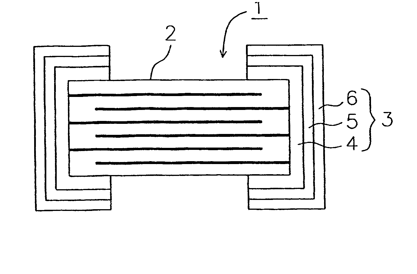
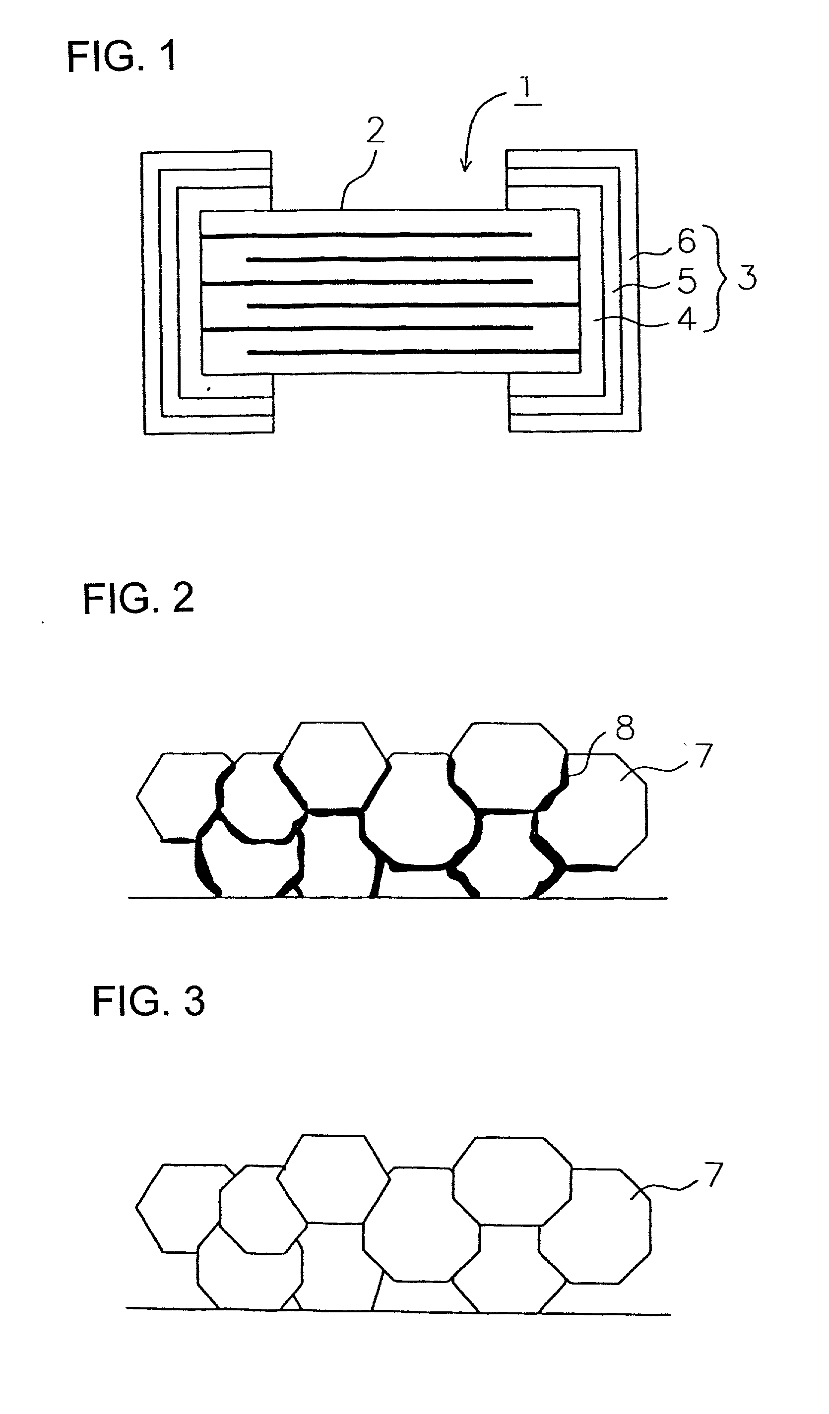
An electronic component includes external electrodes formed on a base member, each external electrode including a plurality of layers of which the outermost layer is a tin plating layer. The tin plating layer has a polycrystalline structure, and atoms of a metal other than tin are diffused into the tin crystal grain boundaries. Alternatively, each external electrode includes a plurality of layers including a thick-film electrode formed on the base member, a nickel layer or a nickel alloy layer formed on the thick-film electrode and a tin plating layer formed on the nickel layer or the nickel alloy layer. The tin plating layer has a polycrystalline structure and nickel atoms are diffused into the tin crystal grain boundaries. Methods for fabricating electronic components and a circuit board provided with a plurality of electronic components are also disclosed.
Description
[0001] 1. Field of the Invention[0002] The present invention relates to the structure of external electrodes of electronic components used for high-density mounting, and more particularly, the invention relates to an electronic component in which tin plating layers are formed as the outermost layers of the external electrodes.[0003] 2. Description of the Related Art[0004] Electronic components, such as chip-type monolithic capacitors, are usually mounted on printed wiring boards, etc., by soldering the external electrodes formed on the exterior of chip base members. In such a case, in order to improve solderability relatively inexpensively, tin plating layers are often formed as the outermost layers of the external electrodes. This is because tin plating layers facilitate soldering as compared with nickel layers and copper layers, and also tin plating layers do not easily cause defects when the electronic components are mounted by reflow soldering, flow soldering, or the like.[0005]...
Claims
Login to View More Application Information
Patent Timeline
 IPC IPC(8): B32B15/01C25D7/00B32B15/04C22F1/00C25D3/30C25D5/00C25D5/12C25D5/48C25D5/50C25D7/12H01G4/12H01G4/228H01G4/232H01G4/252H01G4/30H05K1/18H05K3/34
CPCH01G4/232Y10S428/901Y10T428/12722Y10T428/12944Y10T428/24917Y10T428/265Y10T428/24975Y10T428/12861Y10T428/12535Y10T428/12708C25D3/00
Inventor HIGUCHI, SHOICHI
Owner MURATA MFG CO LTD