Method for removing organic contaminants from a semiconductor surface

a technology for organic contaminants and semiconductors, applied in the direction of photomechanical equipment, cleaning using liquids, instruments, etc., can solve the problems of non-uniform etching and cleaning on the wafer surface, high processing temperature, and high cost of chemicals

Inactive Publication Date: 2002-01-31
INTERUNIVERSITAIR MICRO ELECTRONICS CENT (IMEC VZW)
View PDF1 Cites 60 Cited by
  • Summary
  • Abstract
  • Description
  • Claims
  • Application Information

AI Technical Summary

Problems solved by technology

The semiconductor surface preparation prior to various processing steps such as oxidation, deposition or growth processes, has become one of the most critical issues in semiconductor technology.
In a pre-clean stage, absorbed organic molecules prevent cleaning chemicals from contacting with the wafer surface, thus leading to non-uniform etching and cleaning on the wafer surface.
However, SPM uses expensive chemicals and requires high processing temperatures, and causes problems in terms of chemical waste treatment.
Other sources of organic contamination also arise during a standard IC process flow.
If the polymer is not completely removed prior to the subsequent metal deposition, the polymer will mix with sputtered metal atoms to form a high resistance material resulting in reliability concerns.
These processes are both expensive and environmentally harmful in terms of waste treatment.
However, both oxidation pathways are concurrent and conditions that favor advanced oxidation pathways will occur at the expense of the efficiency of eliminating organic contamination with higher reactivity towards molecular ozone.

Method used


Image

  • Method for removing organic contaminants from a semiconductor surface
  • Method for removing organic contaminants from a semiconductor surface
  • Method for removing organic contaminants from a semiconductor surface

Examples


Embodiment Construction

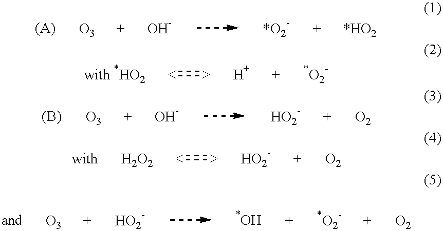
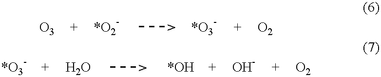
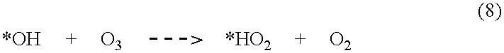
[0057] The purpose of the present invention is related to a method for removing organic contamination from a substrate and / or to a method for oxidizing a silicon wafer. Said substrate can be a semiconductor surface. Said method can be applied for the removal of photoresist and organic post-etch residues from silicon surfaces. Said organic contamination can be a confined layer covering at least part of said substrate. Said confined layer can have a thickness in a range of submonolayer coverage to 1 .mu.m. Said method is applicable for either gasphase or liquid processes.

[0058] In the following specification, a first preferred embodiment of the invention for gas phase processing and a second preferred embodiment for liquid phase processing are described.

[0059] Description of a First Preferred Embodiment for Gasphase Processing

[0060] In said gasphase process, said substrates are placed in a tank such that said substrates are in contact with a gas mixture containing water vapor, ozone a...


PUM

PropertyMeasurementUnit
thicknessaaaaaaaaaa
temperatureaaaaaaaaaa

Abstract

A method for removing organic contaminants from a semiconductor surface whereby the semiconductor is held in a tank and the tank is filled with a fluid such as a liquid or a gas. Organic contaminants, such as photoresist, photoresidue, and dry etched residue, occur in process steps of semiconductor fabrication and at times, require removal. The organic contaminants are removed from the semiconductor surface by holding the semiconductor inside a tank. The method may be practiced using gas phase processing or liquid phase processing. The tank is filled with a gas mixture, a liquid, and / or a fluid, such as water, water vapor, ozone and / or an additive acting as a scavenger (a substance which counteracts the unwanted effects of other constituents of the system).

Description

REFERENCE TO RELATED APPLICATIONS[0001] This application is a continuation-in-part of U.S. patent application Ser. No. 09 / 022,834 filed on Feb. 13, 1998 and claims priority benefits under 35 U.S.C. .sctn.119(e) to U.S. provisional application Serial No. 60 / 040,309, filed on Feb. 14, 1997, to U.S. provisional application Serial No. 60 / 042,389, filed on Mar. 25, 1997, and to U.S. provisional application Serial No. 60 / 066,261, filed on Nov. 20, 1997.[0002] A. Field of the Invention[0003] The present invention is related to a method for removing organic contaminants from a semiconductor surface.[0004] The present invention is also related to the use of this method for a number of applications such as cleaning sequences or cleaning after VIA etching and other etch processes.[0005] B. Description of Related Art[0006] The semiconductor surface preparation prior to various processing steps such as oxidation, deposition or growth processes, has become one of the most critical issues in semic...

Claims


Application Information

Patent Timeline
Patent Type & Authority Applications(United States)
IPC IPC(8): G03F7/42H01L21/306H01L21/311H01L21/768
CPCG03F7/42G03F7/423H01L21/02063H01L21/31116H01L21/31133H01L21/31138H01L21/76814
Inventor DEGENDT, STEFANSNEE, PETERHEYNS, MARCMERTENS, PAULMEURIS, MARC
Owner INTERUNIVERSITAIR MICRO ELECTRONICS CENT (IMEC VZW)
Why Eureka
Try Eureka