Method and apparatus for wiring, wire, and integrated circuit

a technology of integrated circuits and wires, applied in the direction of solid-state devices, coatings, chemical vapor deposition coatings, etc., can solve the problems of increasing interconnection resistance, difficulty in sufficiently plugging the wiring material, and conventional plugging methods not working sufficiently

Inactive Publication Date: 2002-02-21
FUJITSU SEMICON LTD
View PDF0 Cites 10 Cited by
  • Summary
  • Abstract
  • Description
  • Claims
  • Application Information

AI Technical Summary

Problems solved by technology

There is a problem that it is difficult to plug the wiring material sufficiently into the via hole having a large aspect ratio using the conventional PVD method or CVD method. FIG. 7 shows a void formation generated by insufficient deposition method.
However, the conventional plugging method does not work sufficiently, which causes to generate a void 102.
This may further cause a problem to increase interconnect resistance or in a worse case, to generate disconnection.
The problem is brought by poor stepcoverage, i.e., a metal film is made nonuniformly on the side surface of the via hole 10 at an initial stage of d

Method used


Image

  • Method and apparatus for wiring, wire, and integrated circuit
  • Method and apparatus for wiring, wire, and integrated circuit
  • Method and apparatus for wiring, wire, and integrated circuit

Examples


Embodiment Construction

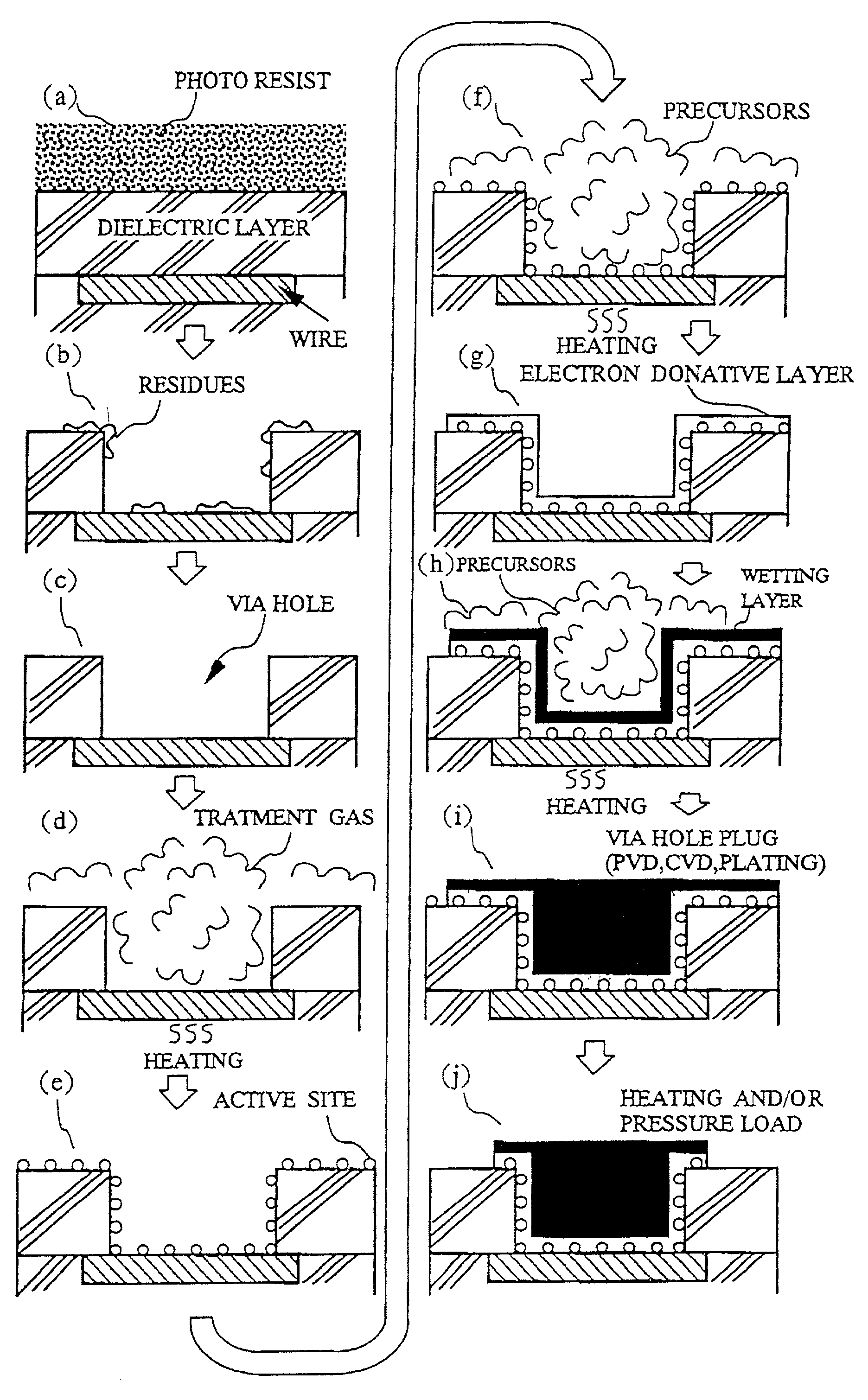
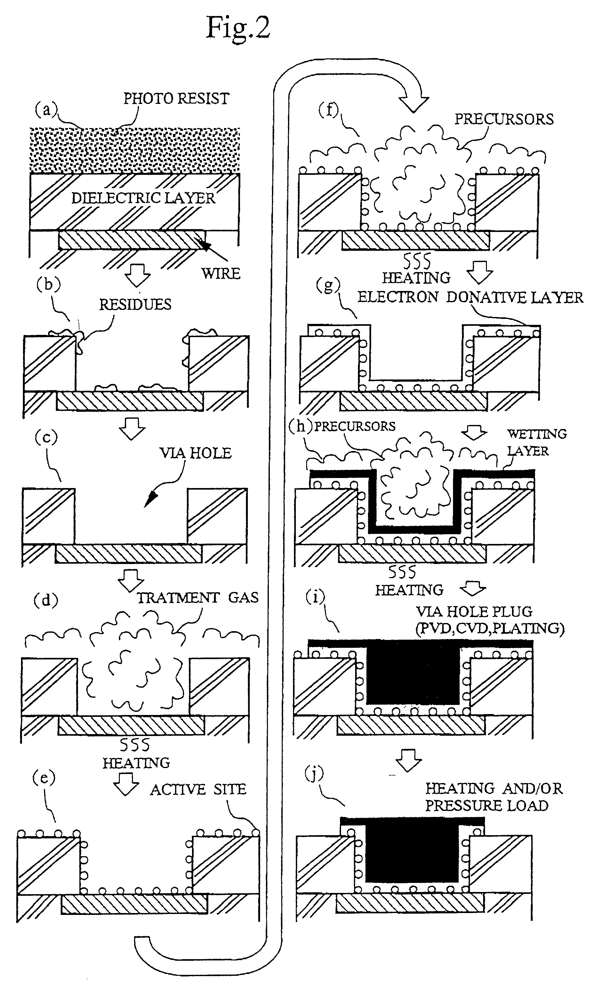
[0026] In the following, one embodiment according to the invention will be described when applied to a producing process of an integrated circuit (hereinafter, referred to as "IC"), for example. can be divided into "front-end process" and "back-end process". "Front-end process" is a process for providing an IC element on the wafer. On the other hand, "back-end process" is a process for electrically connecting the IC elements on the wafer. The present invention can be applied to the "backend process".

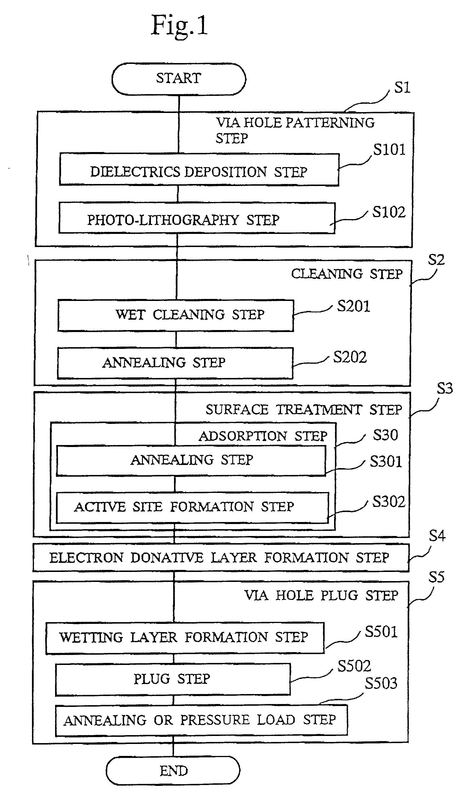
[0027] As shown in FIG. 1, the embodiment according to the invention is performed after a via hole patterning step S1 and a cleaning step S2. The via hole patterning step S1 is provided for producing the via hole in a dielectric layer (a film of dielectronics). Secondly, the cleaning step S2 is provided for removing soil on the wafer such as contaminant and impurities remained after the via hole is patterned.

[0028] The via hole patterning step S1 includes a dielectrics deposition step S1...


PUM

PropertyMeasurementUnit
Densityaaaaaaaaaa
Affinityaaaaaaaaaa

Abstract

The present invention provides a method for wiring, which plugs conductive material sufficiently into a via hole produced in dielectronics (hereinafter, referred to as "a via hole") and prevents generating a void. The via hole is made through a via hole patterning step and a cleaning step. At a surface treatment step, substance having chemical affinity (active site) is adsorbed to the surface of the via hole. Next, an electron donative layer is made by depositing substance having an electron donative characteristic on the active sites acting as cores at an electron donative layer formation step. Then, the wiring material is plugged at a via hole plug step.

Description

[0001] 1. Field of the Invention[0002] The present invention relates to a method and an apparatus for wiring, a wire and an integrated circuit. In particular, the invention relates to, for example, a method and an apparatus for wiring whose material is plugged sufficiently so as to prevent generation of a void or to prevent disconnection, a wire and an integrated circuit having the wire[0003] 2. Description of the Related Art[0004] Recently, semiconductor devices have been integrated so highly that a designing rule of nanometer level has been applied to a design of integrated semiconductor devices instead of the designing rule of micron level (e.g., The National Technology Roadmap for Semiconductors Technology Needs, SIA, 1997 edition). A multi-layered wiring structure including wires made on each layer of multiple layers has been utilized to integrate semiconductor devices. An electric interconnection among these wires made on the multiple layers inserting an interlayer dielectroni...

Claims


Application Information

Patent Timeline
IPC IPC(8): C23C16/02H01L21/28H01L21/285H01L21/77H01L21/768
CPCH01L21/28556H01L21/76802H01L21/76814H01L21/76838H01L21/76843H01L21/76871H01L21/76876H01L21/76877H01L2221/1089H01L21/77
Inventor OHBA, TAKAYUKI
Owner FUJITSU SEMICON LTD
Why Eureka
Try Eureka