Surface emitting semiconductor laser and method of manufacturing the same
a semiconductor laser and surface technology, applied in semiconductor lasers, laser details, optical resonator shape and construction, etc., can solve the problem of difficult to control the shape of the inner edge to be closer to a true circl
- Summary
- Abstract
- Description
- Claims
- Application Information
AI Technical Summary
Benefits of technology
Problems solved by technology
Method used
Image
Examples
first embodiment
[0055] First Embodiment
[0056] A. Device Manufacturing Process
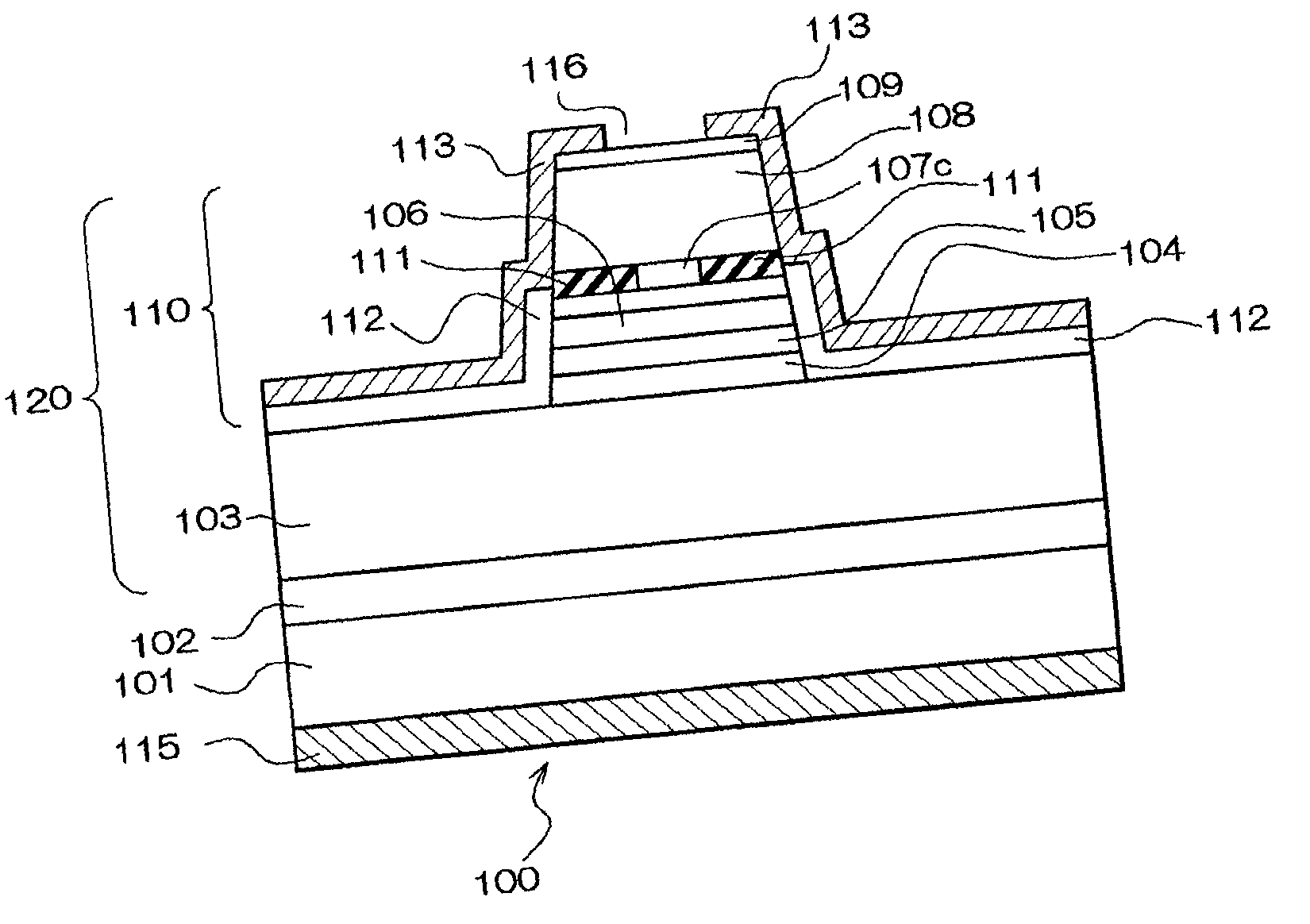
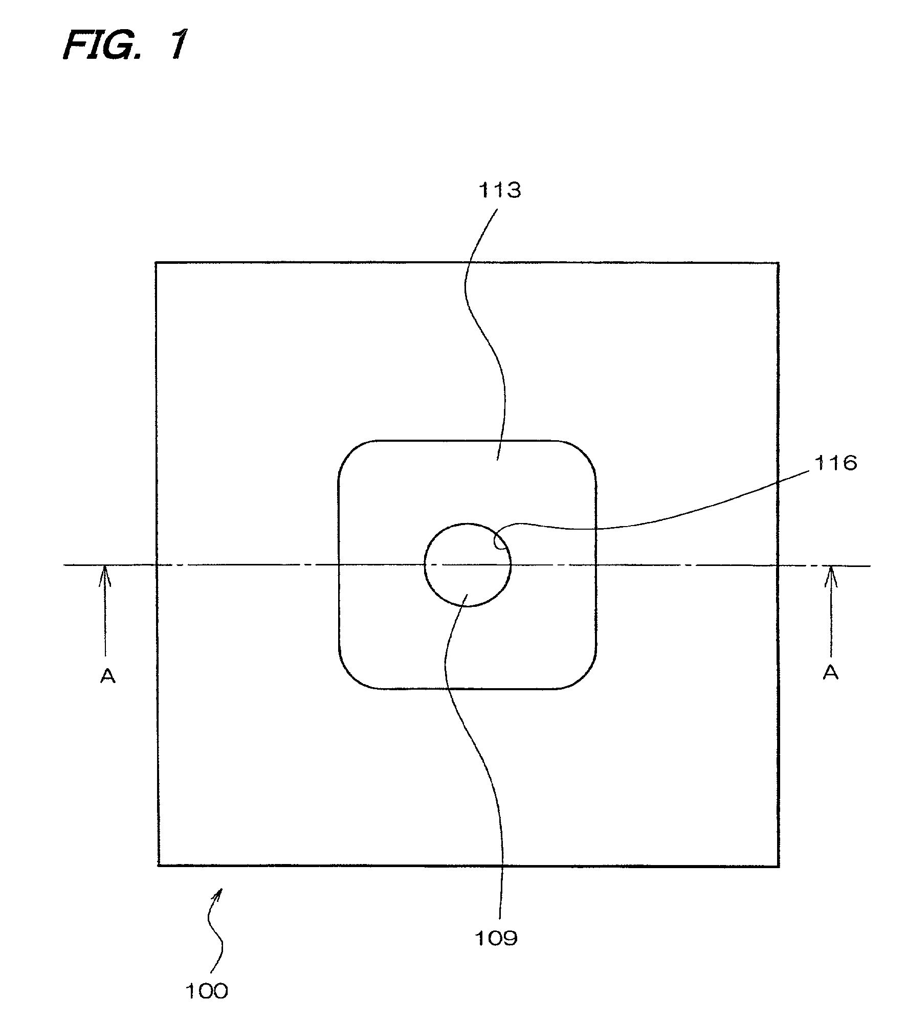
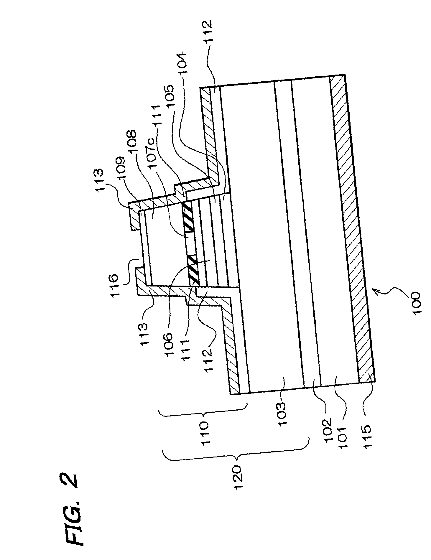
[0057] First, the method of manufacturing the first embodiment of the surface emitting semiconductor laser (referred to hereinafter as "surface emitting laser") 100 of the present invention is described with reference to FIGS. 4 to 7. FIGS. 4 to 6 are sectional views, schematically showing the manufacturing process of a surface emitting laser 100 of this embodiment. FIG. 7 schematically shows a cross-section of a pillar portion 110 formed in the manufacturing process of the first embodiment of the surface emitting laser 100 shown in FIG. 5, in the plane including a current constriction layer formation layer 107a.
[0058] The method of manufacturing the surface emitting laser 100 of this embodiment comprises principally the following steps (a) to (c).
[0059] Step (a) is principally a step of laminating on a semiconductor substrate 101 having Miller indices (100), semiconductor deposition layers 150 including a current constric...
second embodiment
[0095] Second Embodiment
[0096] A. Device Construction
[0097] FIG. 8 is a sectional view, schematically showing a second embodiment of the surface emitting laser 200 of the present invention.
[0098] The surface emitting laser 200 of the second embodiment, as shown in FIG. 8, has substantially the same construction as the first embodiment of the surface emitting laser 100, except that in the plane including the current constriction layer 211, shape of the periphery 240 of a pillar portion 210 other than arc-shaped portions 240a.sub.1, 240a.sub.2, 240a.sub.3, and 240a.sub.4 is curved.
[0099] The surface emitting laser 200 has the pillar portion 210 and current constriction layer 211. The pillar portion 210 and current constriction layer 211 have the same functions as the pillar portion 110 and current constriction layer 111 included in the first embodiment of the surface emitting laser 100.
[0100] Paying attention to the shape of the pillar portion 210, the shape of the periphery 240 of th...
third embodiment
[0105] Third Embodiment
[0106] A. Device construction
[0107] FIG. 9 is a sectional view, schematically showing a surface emitting laser 300 of the third embodiment of the present invention.
[0108] The third embodiment of the surface emitting laser 300 has substantially the same construction as the second embodiment of the surface emitting laser 200, except that on a pillar portion 310 is formed a strain application portion 330 which generates a strain in the active layer (not shown in the drawings). The shape of the periphery 340 of the pillar portion 310, like the pillar portion 210, is constituted by arc-shaped portions 340a.sub.1 , 340a.sub.2, 340a.sub.3, and 340a.sub.4, and curved lines 340b.sub.1, 340b.sub.2, 340b.sub.3, and 340b.sub.4 joining adjacent of the arc-shaped portions. Further, the distance 131 between the arc-shaped portion 311a, and arc-shaped portion 340a.sub.1, the distance 1.sub.32 between the arc-shaped portion 311a.sub.2 and arc-shaped portion 340a.sub.2, the dis...
PUM
 Abstract
Description
Claims
Application Information


