
Stackable microelectronic components with self-addressing scheme

a technology of microelectronic components and self-addressing, which is applied in the field of stackable microelectronic components with self-addressing schemes, can solve the problems of limited memory, increased cost of customized alternatives, and already dense electronic circuitry in the case of most implantable cardiac stimulators

Inactive Publication Date: 2002-05-02
INTERMEDICS
View PDF0 Cites 39 Cited by
  • Summary
  • Abstract
  • Description
  • Claims
  • Application Information

AI Technical Summary

Benefits of technology

This solution enables the addition of memory without expanding the device's area, allowing for increased functionality and memory capacity within the same size constraints, thereby enhancing the performance and longevity of cardiac stimulators while reducing costs.

Problems solved by technology

Although such packages occupy a substantially greater area that the integrated circuit chip itself, most applications are not so size sensitive that the increased expense of customized alternatives is a viable option.
However, due to the size requirements discussed above, electronic circuitry contained in the cases of most implantable cardiac stimulators is already quite densely packed.
Thus, only a limited amount of memory exists to accommodate the various different functions that designers may wish to program into the cardiac stimulator.
As a result, designers must, at times, make difficult decisions regarding the functions that an implantable cardiac stimulator possesses, as well as the manner in which it performs these functions.
Also, as memory arrays grow in size, yield typically decreases, thus increasing the cost of the memory compared to the same amount of memory in smaller arrays.

Method used


Image

  • Stackable microelectronic components with self-addressing scheme
  • Stackable microelectronic components with self-addressing scheme
  • Stackable microelectronic components with self-addressing scheme

Examples


Embodiment Construction

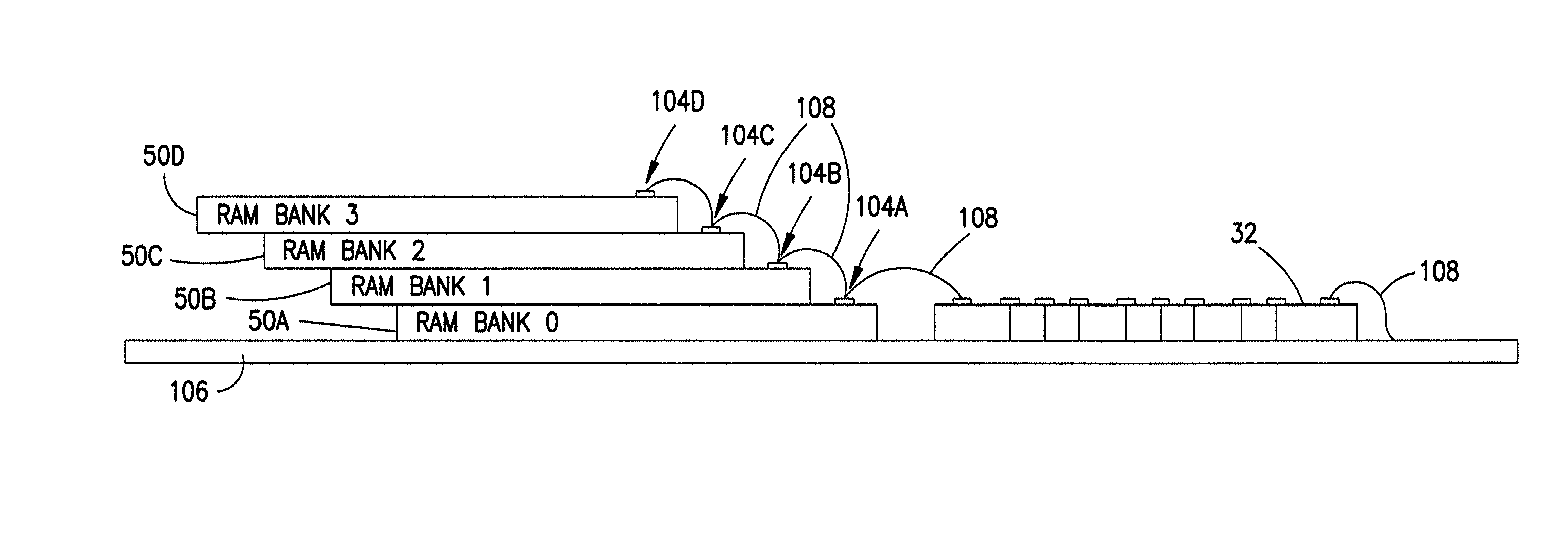
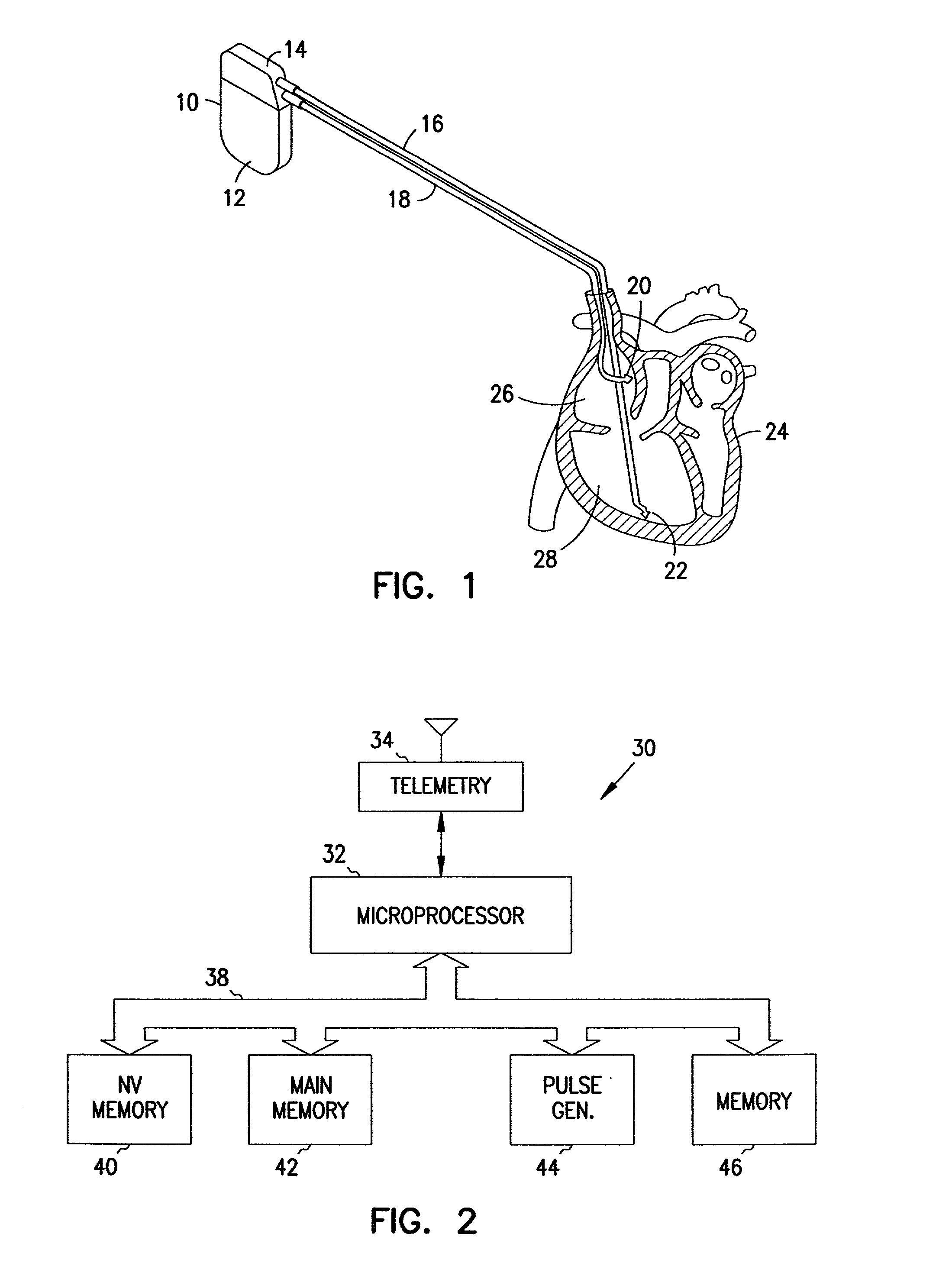
[0023] Turning now to the drawings and referring initially to FIG. 1, one embodiment of a cardiac stimulator is illustrated and generally designated by a reference numeral 10. The cardiac stimulator 10 includes stackable microelectronic components having a self addressing scheme that will be described in detail herein. The illustrated cardiac stimulator 10 is a dual chamber pacemaker, but it should be understood that other types of cardiac stimulators, such as defibrillators and single chamber pacemakers, as well as a variety of other products, may also benefit from these teachings.

[0024] The case of the cardiac stimulator 10 includes a can 12 and a header 14. The cardiac stimulator 10 may be implantable or non-implantable. If implantable, the can 12 and the header 14 are hermetically sealed to prevent bodily fluids from damaging the internal circuitry of the pacemaker 10. Typically, the can 12 is made of titanium, and the header 14 is made of polyethylene.

[0025] Because the illustr...


PUM


Abstract

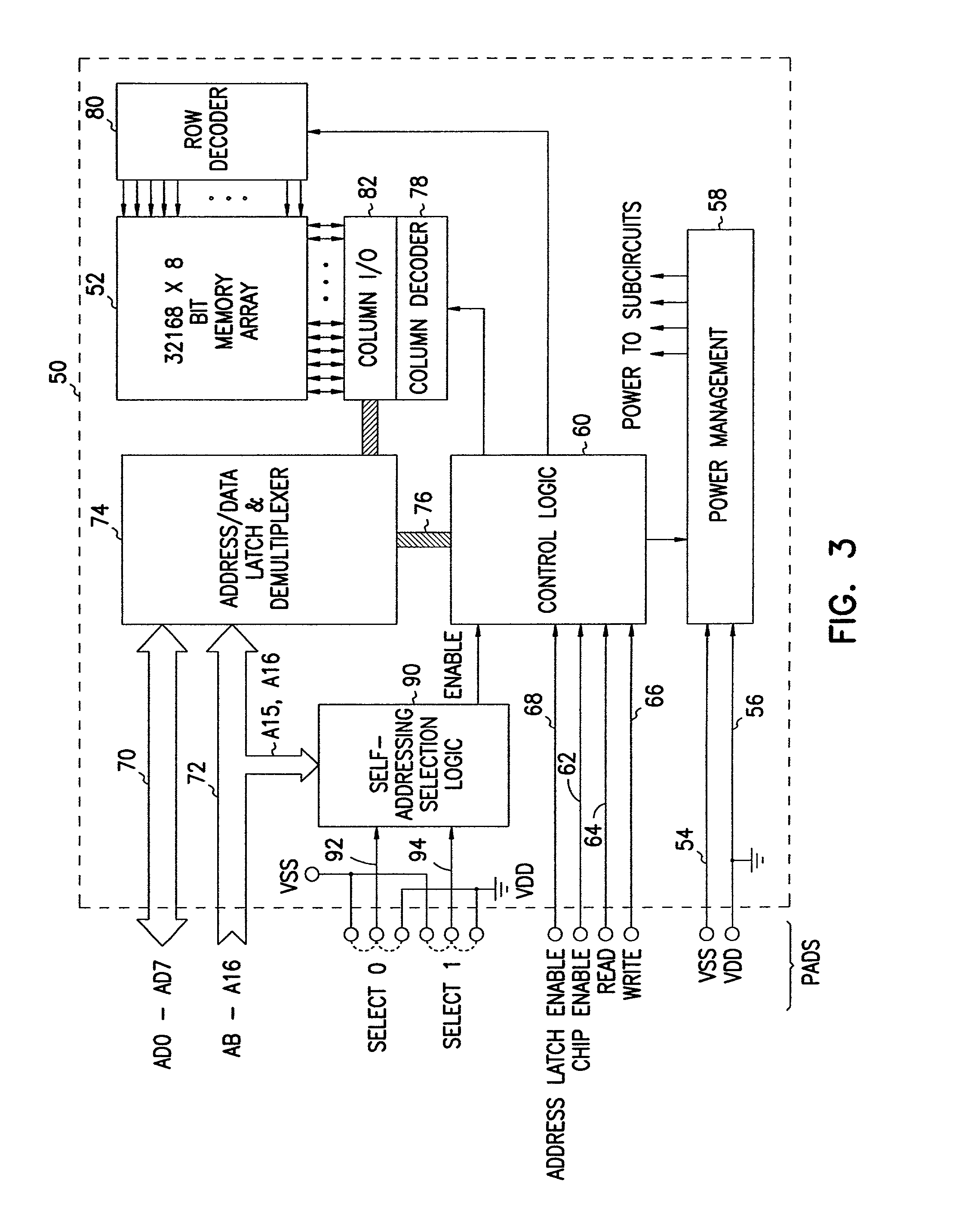
A memory device particularly useful in size-constrained electronic products, such as cardiac stimulators. To provide additional memory for such size-constrained products, memory chips are stacked one on top of another. The memory chips are configured to facilitate bonding without crossed contacts, using aligned bonding pads, vias, or castellations. Each memory chip also includes an address selection circuit that receives signals from one or more address lines to selectively enable and disable the memory chips in the stack.

Description

[0001] This invention relates generally to an addressing scheme for multiple microelectronic components. More particularly, the invention relates to a self-addressing scheme for stackable microelectronic components, such as memory chips. Even more particularly, this invention relates to a self-addressing scheme for stackable microelectronic components used for cardiac stimulators.DESCRIPTION OF THE RELATED ART[0002] With the advent of the transistor a few decades ago and the ensuing developments in integrated circuit technology, electronic circuits have become smaller and smaller. Because the size of the circuits has decreased, the functionality of an electronic circuit of any given size has tended to increase dramatically The microprocessor is largely responsible for this dramatic increase in functionality, so it is no surprise that many of today's electronic circuits operate under microprocessor control. As is well known, microprocessors are essentially generic devices that may be...

Claims


Application Information

Patent Timeline
Patent Type & Authority Applications(United States)
IPC IPC(8): A61N1/362A61N1/375H01L25/065H01L25/07H01L25/18
CPCA61N1/375H01L2224/32145H01L2224/48137H01L2224/48145H01L2224/49175H01L2225/06506H01L2225/0651H01L2225/06555H01L2225/06562H01L2924/14H01L2224/48091H01L2224/73265H01L2224/48227H01L2224/32225H01L2924/01019H01L25/0657H01L2924/00H01L2924/00012H01L2924/00014H01L2224/48147H01L2224/05554H01L24/73A61N1/37512
Inventor PRUTCHI, DAVIDPAUL, PATRICK J.
Owner INTERMEDICS
Learn More