Light emitting diodes with spreading and improving light emitting area

a light emitting diode and spreading current technology, applied in the field of light emitting diodes, can solve the problems of insufficient conductivity of the p-type gan, the difficulty of making p-type ohmic contacts on and spreading current in the p-type gan layer, and the inability to achieve high-conductivity p-type gans, so as to improve the light emitting area, spread current, and enhance the effect of light emitting area

Inactive Publication Date: 2002-09-19
UNI LIGHT TECH INC
View PDF0 Cites 33 Cited by
  • Summary
  • Abstract
  • Description
  • Claims
  • Application Information

AI Technical Summary

Benefits of technology

0008] One of the objectives of the present invention is to provide light emitting diodes with spreading current and improving light emitting area. Multitude of hollow patterns opened on the transparent contact can block the current shortcuts and further spread current and enhance the light emitting area.

Problems solved by technology

However, it is still difficult to prepare a highly conductive p-type GaN layer.
Therefore, it is more difficult to make p-type ohmic contacts on and spread current in the p-type GaN layer.
However, the conductivity of the p-type GaN is still inferior to that of n-type one.
But the arrangement for the contacts has the disadvantage of current crowding happening between these electrodes.
As a result, the light emitting surface is not utilize efficiently, and the lifetimes of the transparent contact and the device are shorten by the current crowding.

Method used


Image

  • Light emitting diodes with spreading and improving light emitting area
  • Light emitting diodes with spreading and improving light emitting area
  • Light emitting diodes with spreading and improving light emitting area

Examples


second embodiment

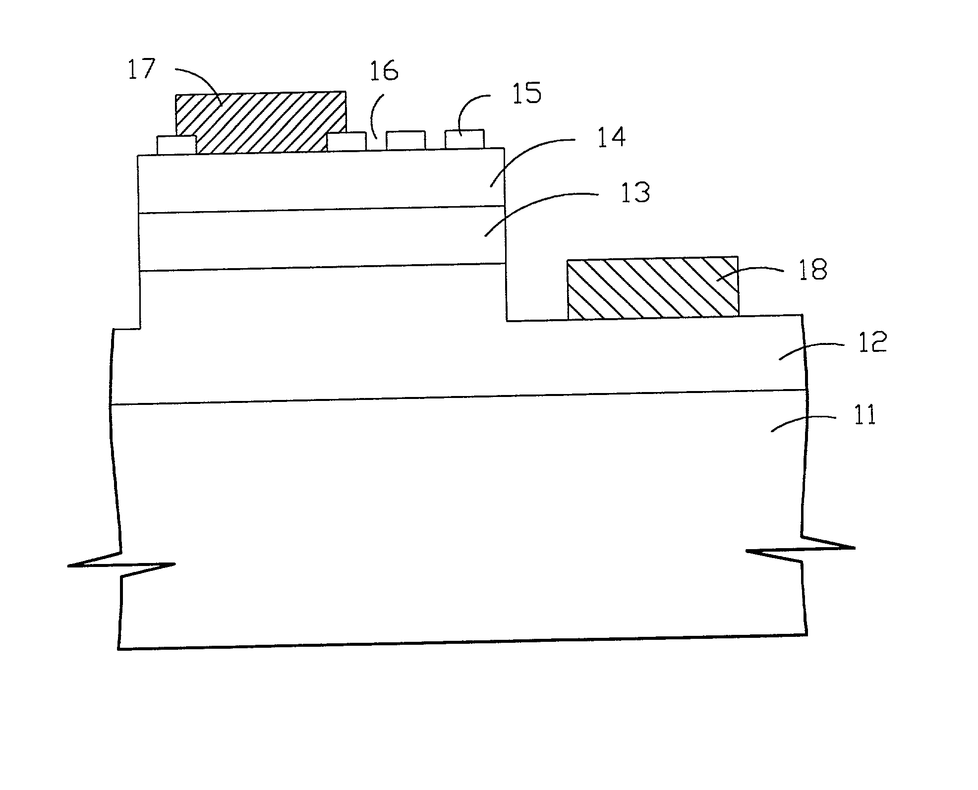
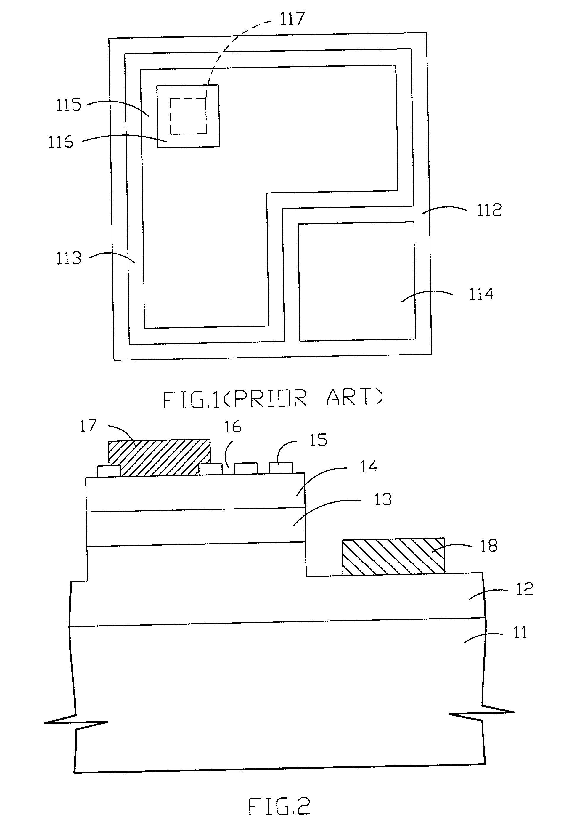
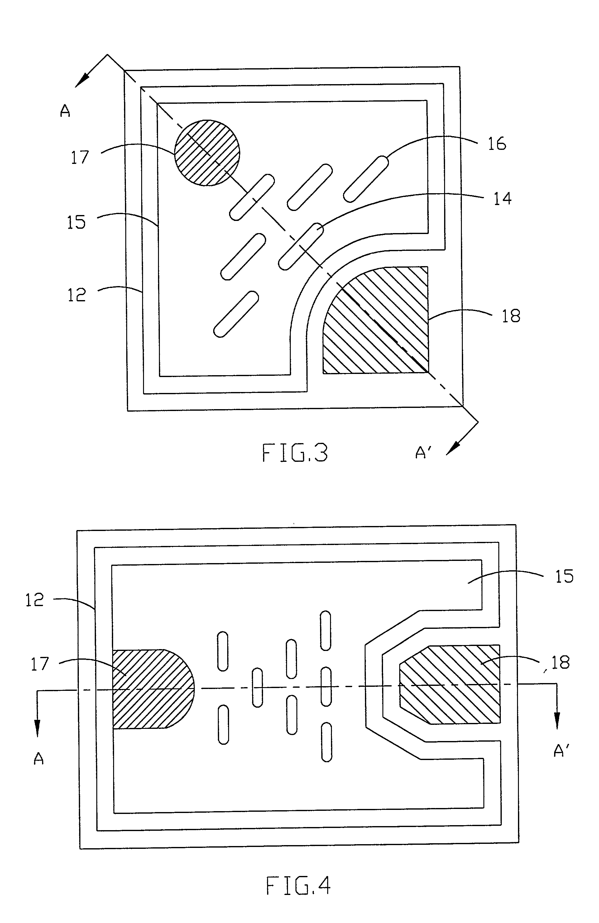
[0031] In the second embodiment, a transparent contact 25, a p-type contact 27, and an n-type contact 28 are on an n-GaN structure 22. They are arranged in such way that the distance from any point of the p-type contact 27 to the n-type contact 28 is the shortest and kept same for each path. The p-type contact 27 has a quarter-circle shape, and the transparent contact 25 has a fan shape that has a same center of the circle as that of the p-type contact 27. The radial distance of spreaded current is all the same from the p-type contact 27 to the n-type contact 28 through the transparent contact 25.

[0032] Depicted in FIG. 7 is another one design of the shapes and arrangements for a p-type contact 37, an n-type contact 38, and a transparent contact 35 on a mesa structure 32 which is on an n-GaN structure 33. The p-type contact 37 and the n-type contact 38 are arranged at the opposite sides rather than the opposite corners. The shapes of the p-type contact 37 and the n-type contact 38 a...

first embodiment

[0033] Again, the current spreading and efficient usage of the lightemitting area is further improved with more symmetrical contact configuration, shown in FIG. 8. In the embodiment, the epi-layer structure is the same as that of the first embodiment, while the shapes of the mesa and contacts are different. A ring-shape n-type contact 48 is around the device and on the n-type GaN-based layer 42, both are located at the bottom of the mesa. A p-type transparent contact 45 is on a p-type GaN-based layer 44 and the p-type GaN-based layer 44 is at the top of the mesa. For spreading the current, a p-type contact 47 is positioned at or near the center of the mesa, and n-type contact 48 has a contact pad and a conduction ring. The shapes and positions for both contacts (47 and 48) provide all current distances between the contacts equal or nearly equal all the way around the mesa. Therefore, the device exhibit good current spreading and high area utility. The shape of the p-type contact 47 ...


PUM


Abstract

The present invention provides a light semiconductor device comprising a substrate and a first semiconductor structure on the substrate. A light emitting structure is on a first portion of the first semiconductor structure. A first contact structure is on a second portion of the first semiconductor structure. The second portion is separated from the first portion of the first semiconductor structure. The first contact structure has a first shape. A second semiconductor structure is on the light emitting structure. A transparent contact is on the second semiconductor structure and has a cut-off portion to expose the portion of second semiconductor structure and a second shape. A second contact structure is on the cut-off portion of the transparent contact. The second contact structure contacting the second semiconductor has a third shape. The second contact structure with the third shape is corresponded to both the transparent contact with the second shape and the first contact structure with the first shape whereby a relationship provides a plurality of current paths with substantially equal distances between the first contact structure and the second contact structure.

Description

BACKGROUND OF THE INVENTION[0001] 1. Field of the Invention[0002] The invention relates to light emitting diodes, and more particularly to light emitting diodes with spreading current and improving light emitting area.[0003] 2. Description of the Prior Art[0004] For photonic semiconductor device, light emitting diode (LED) may be the most commonly recognized because of its application to such a wide variety of products and applications such as scientific equipment, medical equipment and, perhaps most commonly, various consumer products in which LEDs form the light source for various signals, indicators, gauges, clocks, and many other familiar items. Semiconductor sources such as LEDs are particularly desirable as light output devices in such items because of their generally long lifetime, low power requirement, and their high reliability.[0005] Since early 1970s, gallium nitride (GaN)-based material has attracted attentions in applications to light emitters because of its wide bandg...

Claims


Application Information

Patent Timeline
Patent Type & Authority Applications(United States)
IPC IPC(8): H01L33/38H01L33/42
CPCH01L33/20H01L33/385H01L33/42
Inventor WU, BOR-JENYIH, NAE-GUANNCHEN, CHIEN-ANCHEN, NAI-CHUAN
Owner UNI LIGHT TECH INC
Why Eureka
Try Eureka