

Low defect density (Ga, Al, In) N and HVPE process for making same
a technology of defect density and hvpe, which is applied in the direction of crystal growth process, polycrystalline material growth, after-treatment details, etc., can solve the problems of poor lattice-match materials, sapphire used, and the approach has not been satisfactory in yielding useful base structures for device fabrication, etc., to reduce defect density, low defect density, and low defect density
- Summary
- Abstract
- Description
- Claims
- Application Information
AI Technical Summary
Benefits of technology
Problems solved by technology
Method used
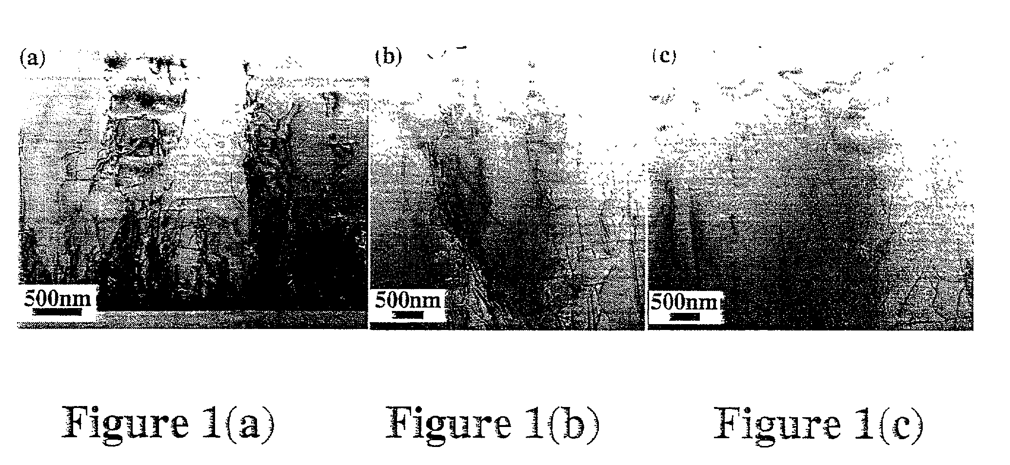
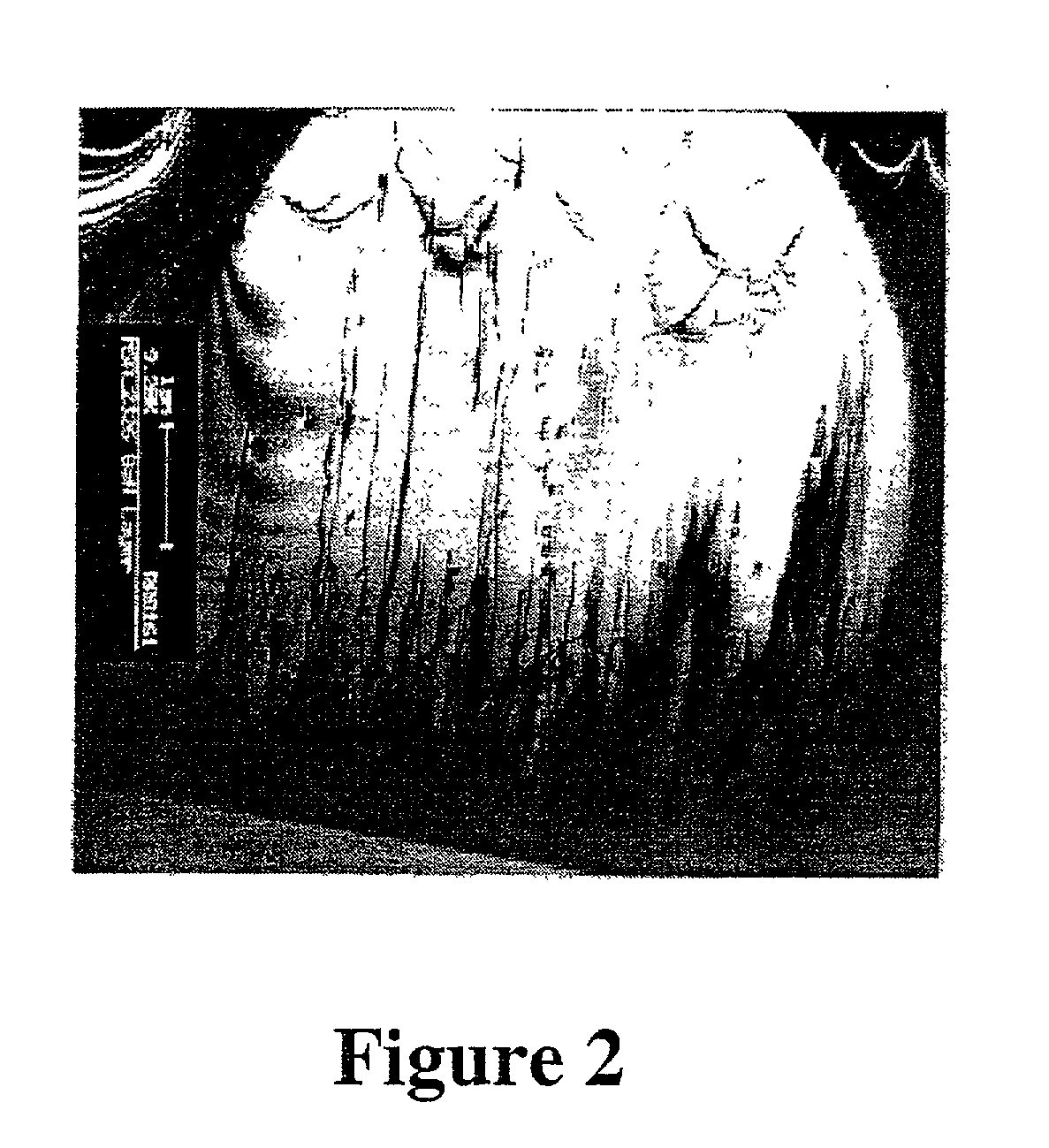
Image

Examples
Embodiment Construction
[0072] The disclosures of the following U.S. Patent Applications, U.S. Patent and literature reference are hereby incorporated herein by reference in their entireties: U.S. provisional patent application No. 60 / 063,249 filed Oct. 24, 1997 in the names of Robert P. Vaudo, Joan M. Redwing, and Vivek Phanse; U.S. application Ser. No. 08 / 984,473 filed Dec. 3, 1997; U.S. provisional patent application No. 60 / 031,555 filed Dec. 3, 1996 in the names of Robert P. Vaudo, Joan M. Redwing, Michael A. Tischler and Duncan W. Brown; U.S. application Ser. No. 08 / 955,168 filed Oct. 21, 1997 in the names of Michael A. Tischler, Thomas F. Kuech and Robert P. Vaudo; U.S. patent application Ser. No. 08 / 188,469 filed Jan. 27, 1994 and issued Oct. 21, 1997 as U.S. Pat. No. 5,679,152.
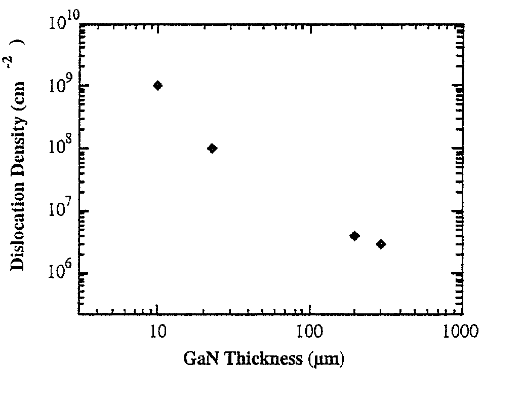
[0073] It will be understood that while the present invention is described hereinafter primarily with specific reference to the formation of GaN, the nitride material alternatively could be formed of other (Ga, Al, In)N speci...
PUM
| Property | Measurement | Unit |
|---|---|---|
| thickness | aaaaa | aaaaa |
| temperature | aaaaa | aaaaa |
| tilt angle | aaaaa | aaaaa |
Abstract
Description
Claims
Application Information