Semiconductor device

a technology of semiconductors and devices, applied in the association of printed circuit non-printed electric components, solid-state devices, basic electric elements, etc., can solve the problems of increasing the cost of chips, the requirement to be met by media apparatuses such as short delivery time and low cost cannot be currently met, and the cost of conventional technology is increased. , the problem of longer processing tim

Inactive Publication Date: 2002-11-14
SEIKO EPSON CORP
View PDF0 Cites 31 Cited by
  • Summary
  • Abstract
  • Description
  • Claims
  • Application Information

AI Technical Summary

Problems solved by technology

However, the development of a system LSI requires a long development time and results in an increased cost of the chip because of mixing of processes of different types.
For this reason, requirement...

Method used


Image

  • Semiconductor device
  • Semiconductor device
  • Semiconductor device

Examples


first embodiment

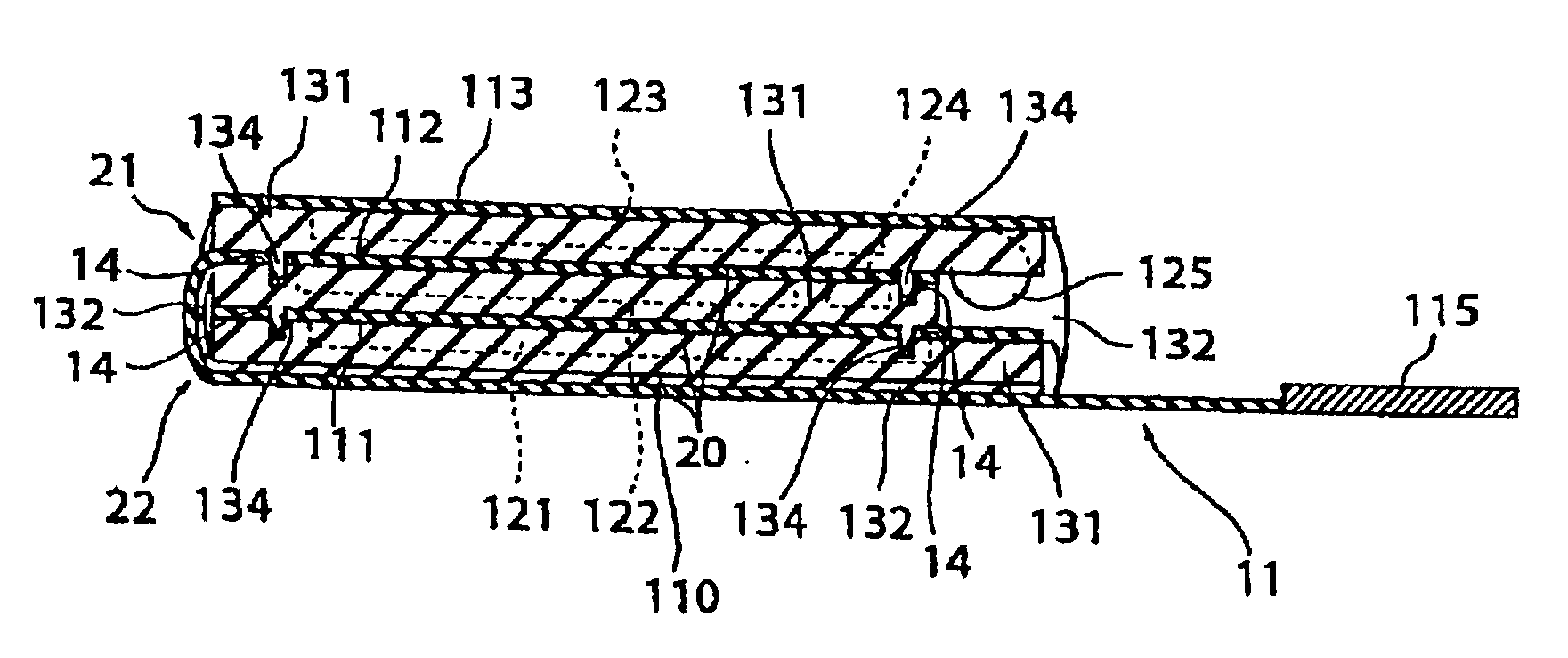
[0012] FIG. 1 shows a prospective view of a structure of a semiconductor device in accordance with the present invention.

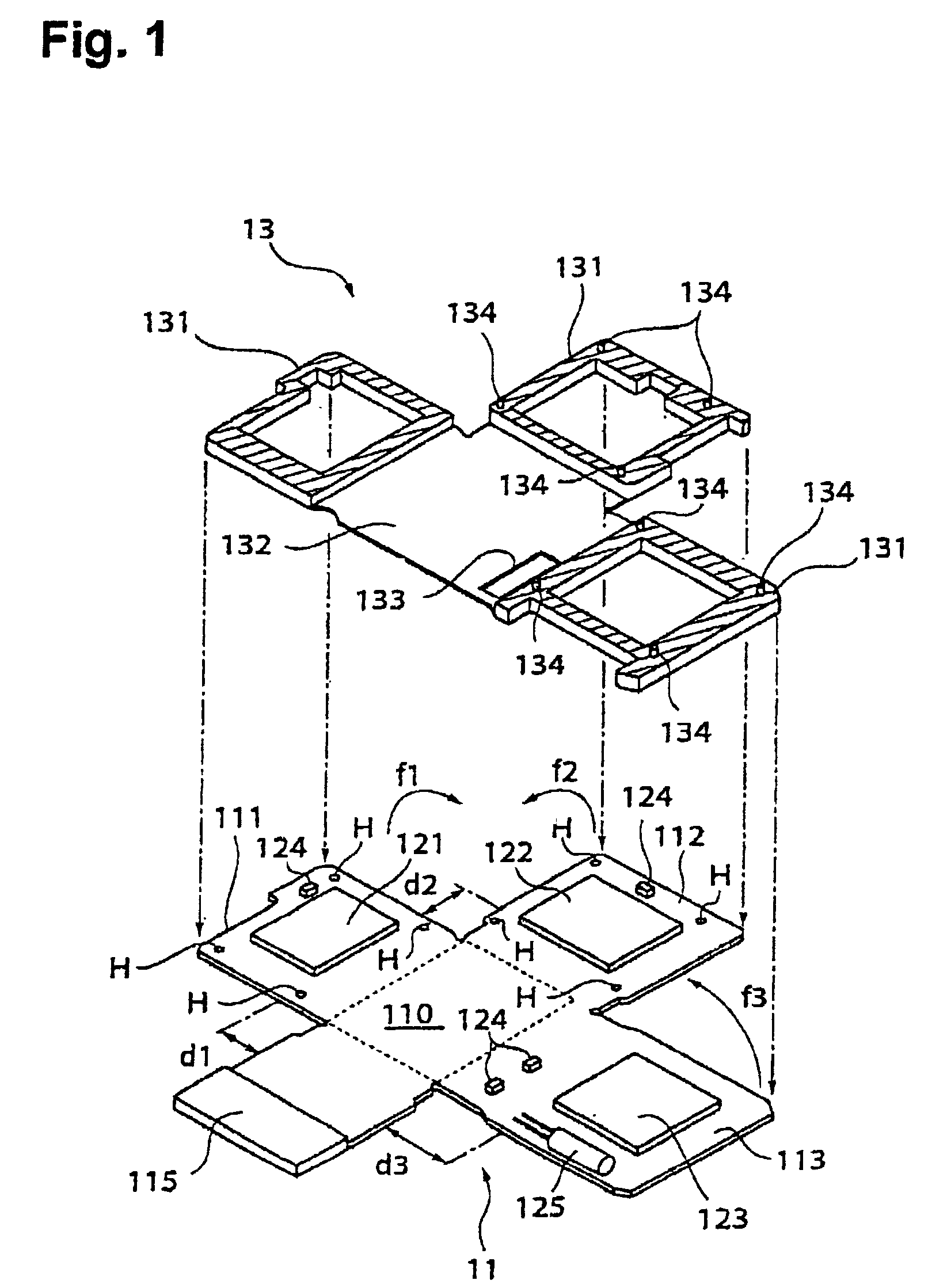
[0013] FIG. 2 shows a perspective view of a characteristic assembling configuration with the structure shown in FIG. 1.

[0014] FIG. 3 shows a cross-sectional view of an assembled configuration of the semiconductor device of FIG. 1.

second embodiment

[0015] FIGS. 4(a) and (b) show a structure of a semiconductor device in accordance with the present invention, respectively, wherein FIG. 4(a) shows a plan view before assembly, and FIG. 4(b) schematically shows a cross-sectional view of a characteristic general structure of a three-dimensional mounting module after assembly.

third embodiment

[0016] FIGS. 5(a) and (b) show a structure of a semiconductor device in accordance with the present invention, wherein FIG. 5(a) shows a plan view before assembly, and FIG. 5(b) schematically shows a cross-sectional view of a characteristic general structure of a three-dimensional mounting module after assembly.

EMBODIMENTS OF THE PRESENT INVENTION IN BEST MODE

[0017] FIG. 1 shows a prospective view of a structure of a semiconductor device in accordance with a first embodiment of the present invention. FIG. 2 shows a perspective view of a characteristic assembly configuration with the structure shown in FIG. 1. As shown in FIG. 1, a flexible circuit substrate 11 has a generally square base region 110 indicated by broken lines, mounting regions 111, 112 and 113 that are continuously provided along the periphery of the base region 110, and predetermined conduction patterns (not shown) formed below a protection film. Also, an external terminal section 115 is provided at the periphery of ...


PUM


Abstract

To provide a semiconductor device with a three-dimensional mounting module using a flexible circuit substrate which is easy to assemble a three-dimensional structure and is excellent in the workability in repair work (or re-work). [MEANS FOR SOLUTION] A flexible circuit substrate 11 has mounting regions 111, 112 and 113 on which electronic components 121, 122 and 123 are mainly mounted, respectively, and other electronic components 124 and 125 are also mounted. The flexible circuit substrate 11 is structured in such a manner that the mounting regions 111~113 are folded on top of the other over the base region 110 in a predetermined order (f1~f3). An integrated spacer 13 has thick regions 131 and thin regions 132, and is superposed and affixed to the flexible circuit substrate 11 as indicated by arrows with broken lines, and supports the electronic components 121~125 stacked in layers. Fixing bosses 134 and aperture sections 14 to be coupled therewith are provided to facilitate positioning.

Description

[0001] The present invention relates to a semiconductor device using a flexible circuit substrate, and more particularly to a semiconductor device composing a three-dimensional mounting module that is required to be inexpensive, smaller in size, and lighter in weight.BACKGROUND TECHNOLOGY[0002] Flexible circuit substrates have the advantage of being soft and deformable unlike rigid circuit substrates. Accordingly, they are advantageous in high-density mounting of ICs and size-reduction of modules. In other words, flexible circuit substrates are used for TCP (tape carrier packages), COF (Chip On Flexible or Film) and the like, and particularly they are indispensable for reducing the size of a variety of media apparatuses.[0003] Also, the system LSI technology is important in the realization of smaller, thinner and lighter media apparatuses. System LSIs are steadily advancing the technology towards the implementation of one-chip while incorporating LSIs of peripheral circuits. However...

Claims


Application Information

Patent Timeline
IPC IPC(8): H05K1/02H01L21/60H01L23/12H01L23/52H01L23/538H01L25/065H01L25/07H01L25/18H05K1/18
CPCH01L23/5382H01L23/5387H01L25/0657H01L2224/16H01L2225/06579H01L2225/06586H05K1/189H01L2225/06575
Inventor KONDO, YOICHIRO
Owner SEIKO EPSON CORP
Why Eureka
Try Eureka