Display device and method of manufacturing the same

a technology of light-emitting elements and display devices, which is applied in the direction of organic semiconductor devices, semiconductor devices, instruments, etc., can solve the problems of increasing the number of dark spots, reducing the display quality, and deteriorating phenomena of organic light-emitting elements

Inactive Publication Date: 2002-12-05
SEMICON ENERGY LAB CO LTD
View PDF6 Cites 262 Cited by
  • Summary
  • Abstract
  • Description
  • Claims
  • Application Information

AI Technical Summary

Problems solved by technology

However, various deterioration phenomena are observed in the organic light-emitting element.
For example, the dark spot, which is a non-light emitting point defect appearing in a pixel portion, is regarded as a problem that remarkably reduces the display quality.
It is said that the dark spot is a progressive defect and the mere presence of water increases the number of dark spots even if the organic light-emitting element is not operated.
The placement of the film sheet 305 or the like increases the distance between the element substrate and the sealing substrate, making it difficult to reduce the thickness of the display device.
Moreover, the thinner the element substrate becomes, the lower the shock resistance becomes.
As a result, the element substrate is likely to be fragile.
In particular, when the sealing substrate made of metal and the element substrate made of glass are bonded to each other, the distortion is generated by a sudden change in temperature due to the difference in thermal expansion coefficient, causing the cracking in the element substrate.
0%. Although the amount of water penetrating into the sealed regio

Method used


Image

  • Display device and method of manufacturing the same
  • Display device and method of manufacturing the same
  • Display device and method of manufacturing the same

Examples


embodiment 1

[0117] (Embodiment 1)

[0118] The present invention is applicable to any display devices using the organic light5 emitting element. FIG. 10 shows an example of such display devices, illustrating an active-matrix display device manufactured by using TFTs. The TFTs in Embodiments are sometimes classified into amorphous silicon TFTs and polysilicon TFTs, depending on the material of a semiconductor film forming a channel formation region. The present invention is applicable to either of them if the channel formation region has a sufficiently high mobility.

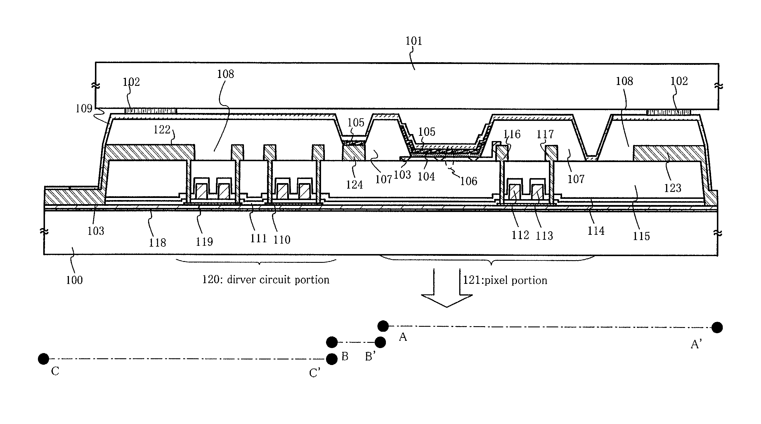
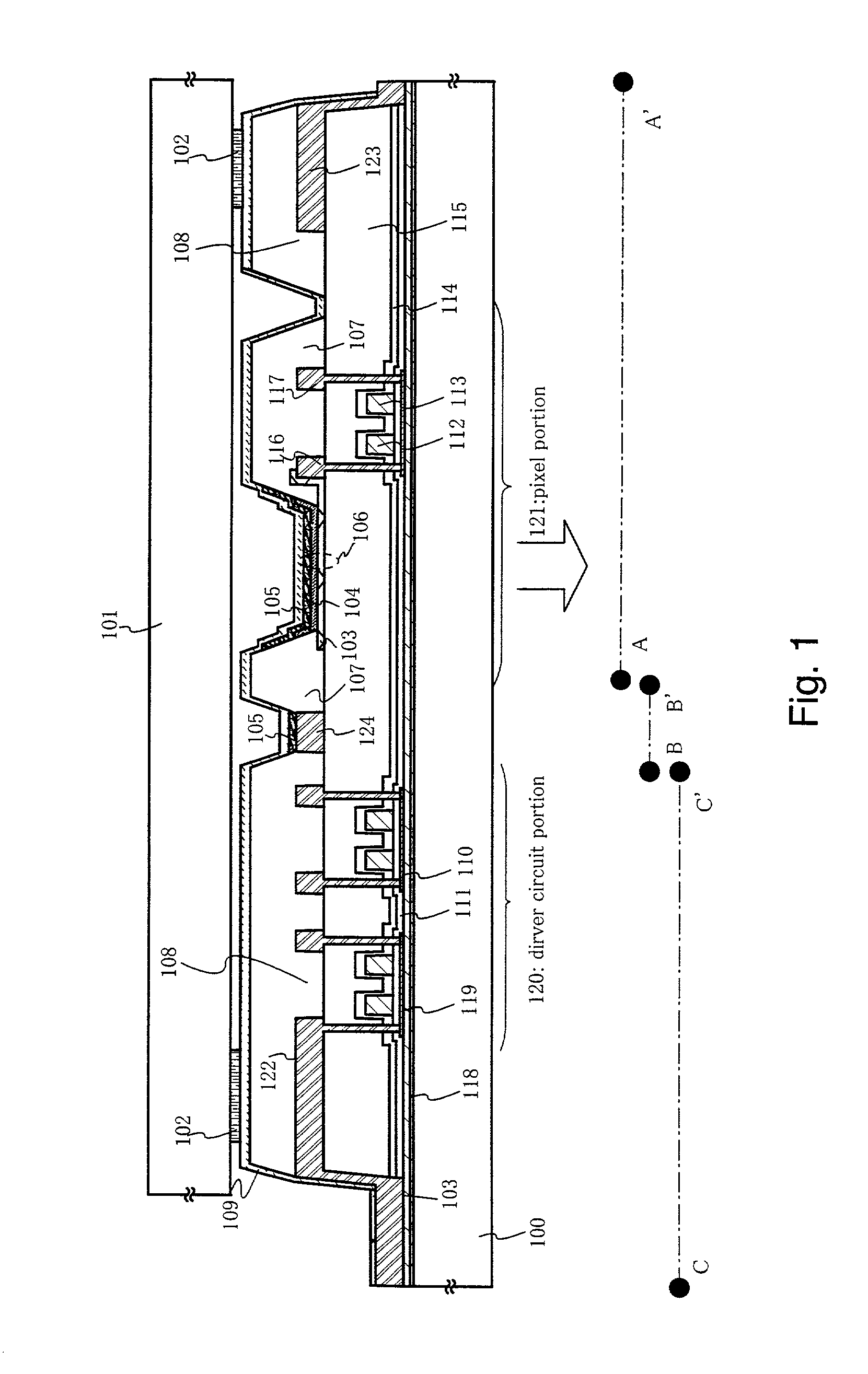
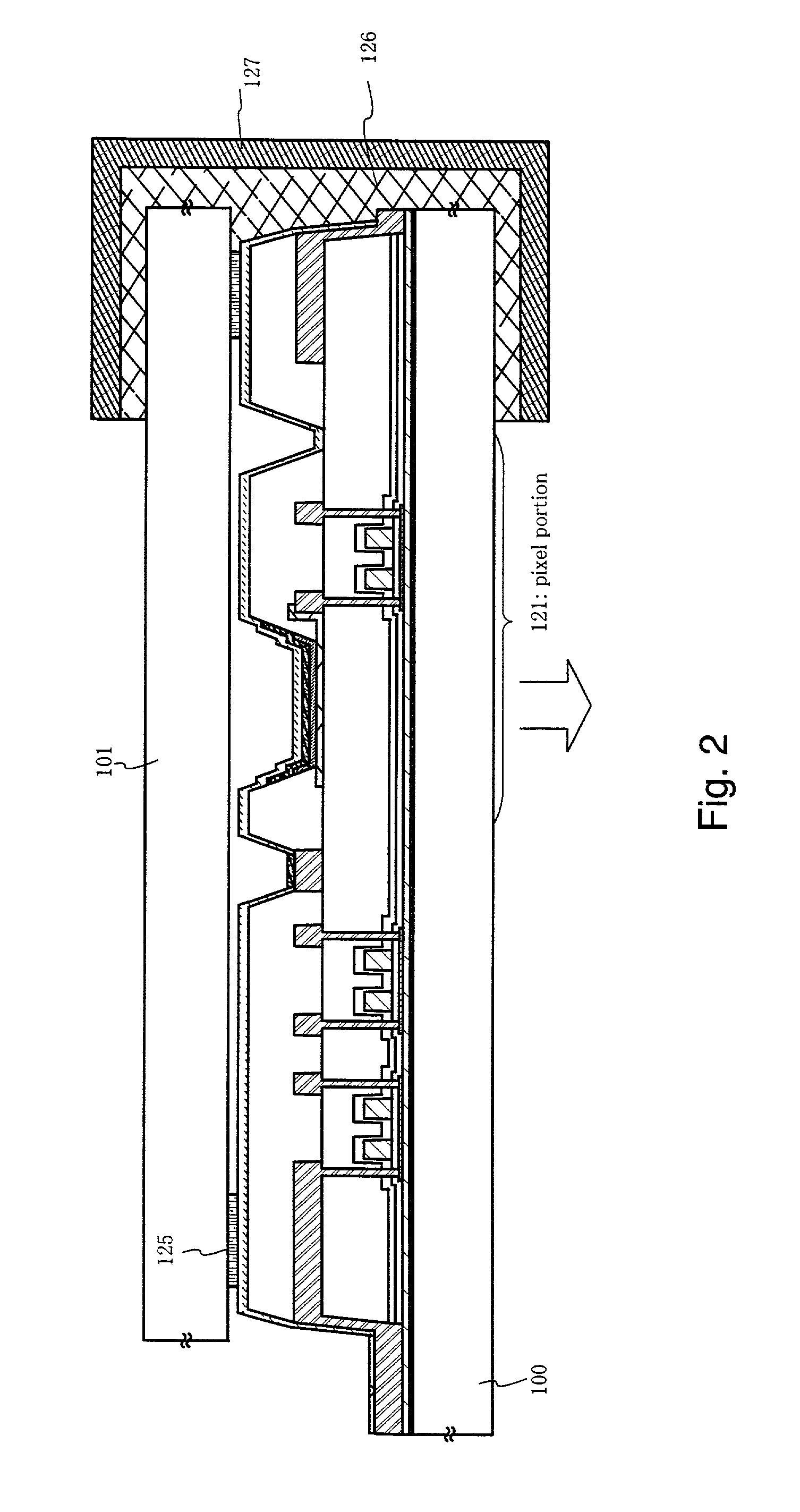
[0119] An n-channel type TFT 431 and a p-channel type TFT 432 are formed in a driving circuit portion 437. A TFT 433 for switching, a TFT 434 for reset, a TFT 436 for current control and a storage capacitor 435 are formed in a pixel portion 438.

[0120] As a substrate 401, a substrate made of glass such as quartz, barium borosilicate glass as is represented by #7059 glass and #1737 glass manufactured by Corning Inc., or alumino borosilica...

embodiment 2

[0139] (Embodiment 2)

[0140] In Embodiment 2, mother substrates (mother glasses), the area of each mother substrate corresponding to the total area of a plurality of unit panels, are bonded to each other. When the mother substrates are cut into individual panels, a CO.sub.2 laser is used as cutting means.

[0141] A CO.sub.2 laser employs carbon dioxide as a reactive medium, and is operated by exciting carbon dioxide to be in an inverted population state. Since the CO.sub.2 laser generates light having a wavelength in an infrared region (10.6 nm), the object irradiated with laser light can be heated.

[0142] A method of cutting a glass substrate using a CO.sub.2 laser will be described with reference to a perspective view of FIG. 14. FIG. 14 is a perspective view showing a method of cutting a glass substrate 501 irradiated with laser, of the glass substrates 501 and 502 that are bonded to each other. An ellipsoidal laser beam spot 503 is radiated onto the glass substrate 501 moving in the...

embodiment 3

[0145] (Embodiment 3)

[0146] A light-emitting device formed by implementing the present invention can be incorporated to various electric-equipment, and a pixel portion is used as an image display portion. Given as such electronic equipment of the present invention are cellular phones, PDAs, electronic books, video cameras, lap-top computers, and image play back devices with the recording medium, for example, DVD (digital versatile disc), digital cameras, and the like. Specific examples of those are shown in FIGS. 12A to 13C.

[0147] FIG. 12A shows a cellular phone, which is composed of a display panel 9001, an operation panel 9002, and a connecting portion 9003. The display panel 9001 is provided with a display device 9004, an audio output portion 9005, an antenna 9009, etc. The operation panel 9002 is provided with operation keys 9006, a power supply switch 9007, an audio input portion 9008, etc. The present invention is applicable to the display device 9004.

[0148] FIG. 12B shows a m...


PUM


Abstract

The object of the present invention is to propose a structure of a display device in which water is prevented from passing through the side faces of a display device using an organic light-emitting element and a gap between substrates is made uniform. On the first substrate having the light-emitting element provided thereon, the thicknesses of the layers deposited in the peripheral area, the pixel portion and the driving circuit portion are equalized with each other. Furthermore, an adhesive is provided as thin as possible in the peripheral area of the first substrate so as to bond a second substrate to the first substrate. As a result, the distance between the first substrate and the second substrate can be made uniform throughout the peripheral area of the first substrate, the pixel portion and the driving circuit. Moreover, since a protective film overlying the organic light-emitting element is also provided on the side faces of the second insulating film, water is prevented from entering the display device through its side faces.

Description

[0001] 1. Field of the Invention[0002] The present invention relates to a display device using an organic light-emitting element and a manufacturing method thereof. More specifically, the present invention relates to a sealing structure for protecting an organic light emitting element deposited onto a substrate, and to a display device, in which an element substrate (a substrate having at least an element such as a TFT) and a sealing substrate are provided in the proximity, and a manufacturing method thereof.[0003] Throughout the specification, the term "organic light-emitting element" indicates an element including an organic compound film sandwiched between two electrodes to achieve light emission. One of the representative organic light-emitting elements is a light-emitting element using an organic light-emitting diode (OLED). The OLED includes an organic compound film sandwiched between two electrodes. Holes are injected to one of the electrodes while electrons are injected to t...

Claims


Application Information

Patent Timeline
IPC IPC(8): H01L27/32H01L51/52H01L51/56
CPCH01L27/3246H01L51/5246H01L51/525H01L2251/558H01L51/56H01L2251/5315H01L51/5253H10K59/122H10K50/8426H10K50/8428H10K50/844H10K71/00H10K2102/3026H10K2102/351
Inventor YAMAZAKI, SHUNPEIKOYAMA, JUNNISHI, TAKESHISATAKE, RUMO
Owner SEMICON ENERGY LAB CO LTD
Why Eureka
Try Eureka