Semiconductor memory device post-repair circuit and method

a memory device and memory chip technology, applied in the field of post-repair structures and methods, can solve the problems of many--even the most--main memory cell arrays on a given wafer may fail to achieve 100% operability, defects may arise, first become apparent,

Inactive Publication Date: 2003-07-03
SAMSUNG ELECTRONICS CO LTD
View PDF2 Cites 117 Cited by
  • Summary
  • Abstract
  • Description
  • Claims
  • Application Information

AI Technical Summary

Problems solved by technology

In practice, many--even most--main memory cell arrays on a given wafer may fail to achieve 100% operability.
Although most memory array defects are detectable during wafer state testing, some defects may arise--or first become apparent--after a memory device is packaged.
Laser-cut fuses do not have post-repair capability, as the packaging material prevents laser targeting and fuse cutting.
Although post-repair redundancy is attractive because it allows the correction of defects that arise during packaging, such redundancy does have drawbacks.
Therefore, the cost of using electrically cut fuses rather than laser-cut fuses, in terms of wafer surface area, may outweigh the benefit of a post-repair capability.
If a redundant memory line that is dedicated for post repair is itself defective, post repair becomes impossible.
This is true even if good redundant laser-repair memory lines remain unused, as those lines cannot be used for post repair.

Method used


Image

  • Semiconductor memory device post-repair circuit and method
  • Semiconductor memory device post-repair circuit and method
  • Semiconductor memory device post-repair circuit and method

Examples


first embodiment

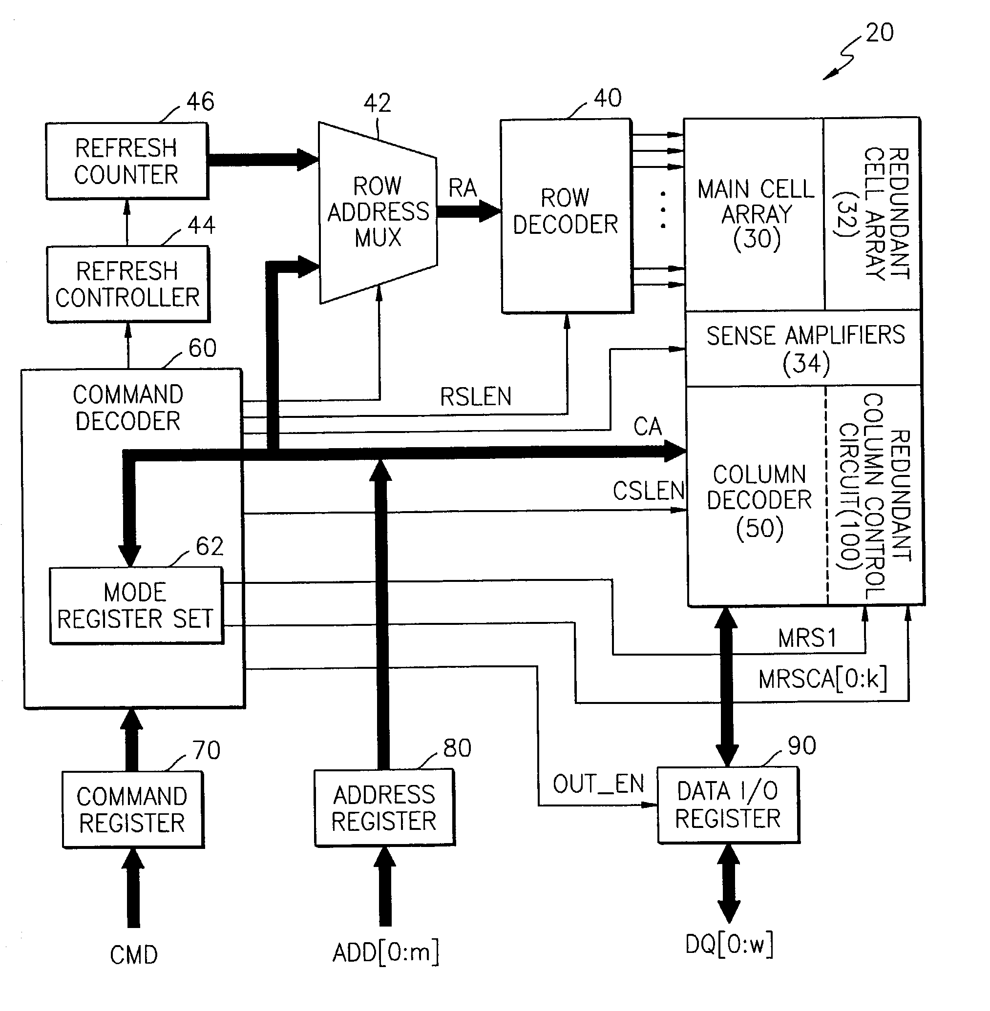
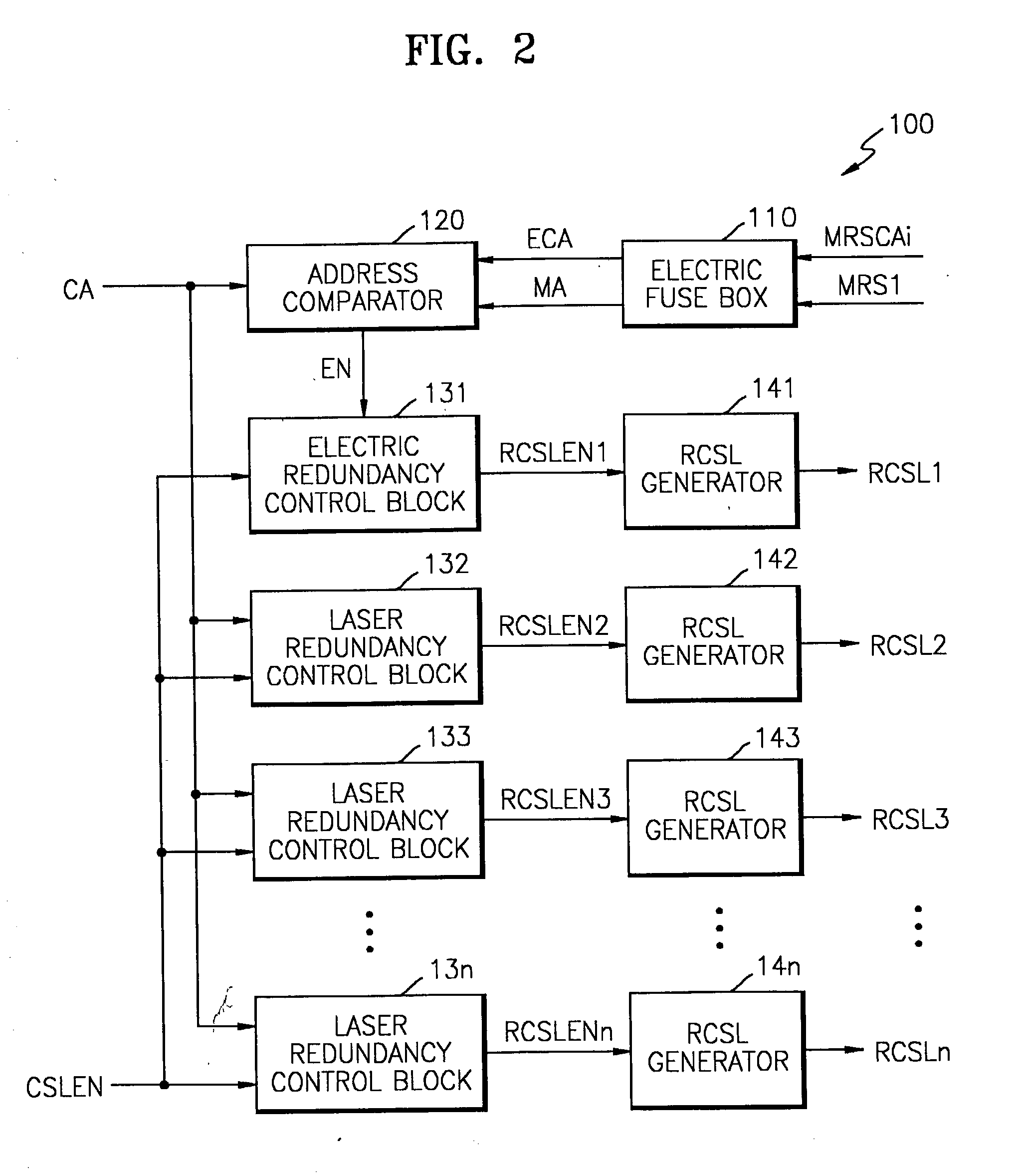
[0030] FIG. 1 illustrates a block diagram for a semiconductor memory device 20--in this case a synchronous DRAM (SDRAM)--according to a Briefly, a main cell array 30 and redundant column cell array 32 are served by row and column circuitry. The column circuitry comprises sense amplifiers 34 and column decoder 50. Column decoder 50 selects, for each column address CA, the column (bit) line(s) that will be read / written to. Within column decoder 50, redundant memory line control circuit 100 determines when a redundant column will be substituted for a main column, based on column address CA and column select enable CSLEN.

[0031] The row circuitry comprises row decoder 40 and row address multiplexer 42. Row decoder 40 selects, for each row address RA, which row (word) line will be activated. Row select enable RSLEN indicates when RA is valid. Although no redundant row lines and circuitry are shown in device 20, such may exist and would be similar to redundant array 32 and control circuit...

second embodiment

[0052] One condition that the embodiment of FIG. 2 cannot correct for is a failure in the redundant column associated with the electric redundancy control block 131. Were this redundant column to be defective, post repair would be impossible, even if one or more of redundant columns 2 through n were defect-free and unused. In contrast, the second embodiment increases the likelihood that post repair will be possible, by allowing the potential selection of one of several redundant columns for association with electrical redundancy control signals. Preferably, then, a defect-free redundant column can be allocated to post-repair after wafer fabrication. And also preferably, each defect-free redundant column can be, in the alternative, allocated to laser repair.

[0053] FIG. 7 illustrates redundant column control circuit 200 of the second embodiment. Although similar to FIG. 2 in some ways, FIG. 7 contains post-repair control blocks 251 to 25n, different redundancy control blocks 231 to 23...

embodiment 900

[0083] Although the preceding embodiments have illustrated circuits that allow a single post-repair operation, the invention is not so limited. For instance, FIG. 14 contains a block diagram for a repair circuit embodiment 900 capable of performing two post-repair operations. Repair circuit 900 has redundancy control blocks 931 through 93n, RCSL generators 941 through 94n, and post-repair control blocks 951 through 95n, similar to the post-repair circuit 200 shown in FIG. 7. However, repair circuit 900 has two electric fuse boxes 911 and 912 and two address comparators 921 and 922, unlike the post-repair circuit 200.

[0084] The two electric fuse units, 911 and 912, are separately programmable through mode register set signals MRS1 and MRSCAi. Note that one mode register set signal can be used by the electric fuse units to gate the remaining mode register set signals, such that each electric fuse unit can be programmed independently.

[0085] Fuse unit 911 generates a first electric colu...


PUM


Abstract

The ability to repair defective cells in a memory array, by replacing those cells with redundant cells, is improved using a redundant memory line control circuit that employs two types of redundancy programming. Most, or all, redundant memory lines can be programmed while the memory array is in a wafer state by, e.g., cutting laser fuses. But at least one memory line can be programmed subsequent to device packaging ("post repair") using, e.g., commands that cut electric fuses. Preferably, the redundant memory line(s) that are reserved for post repair are selectable among the same redundant memory lines that can be programmed using laser fuses. This allows all redundant memory lines to be available for laser repair, if needed, but also allows a redundant memory line to be selected for post repair after it has been determined that that redundant memory line is defect-free. This increases the likelihood that a device will be repairable, and yet does not unnecessarily waste redundant memory lines by pre-dedicating them to laser or post repair.

Description

[0001] 1. Field of the Invention[0002] The present invention pertains generally to semiconductor memory device repair structures and repair methods, and more particularly to post-repair structures and methods.[0003] 2. Description of the Related Art[0004] Semiconductor memory devices, e.g., Dynamic Random Access Memory (DRAM) devices, contain a plurality of memory cells arranged in a row / column array. Each memory cell typically stores one bit of information. The array contains row signal lines, and column signal lines arranged perpendicular to the row lines. A memory cell is placed at each intersection of a row line and a column line. Concurrently addressing the array row line and the array column line that connect to a particular memory cell accesses that memory cell.[0005] Most uses for semiconductor memory devices require that 100% of the memory cells, row lines, and column lines be operational. In practice, many--even most--main memory cell arrays on a given wafer may fail to ac...

Claims


Application Information

Patent Timeline
Patent Type & Authority Applications(United States)
IPC IPC(8): G11C29/00
CPCG11C29/785G11C29/00
Inventor JANG, SEONG-JINKIM, KYU-HYOUN
Owner SAMSUNG ELECTRONICS CO LTD
Why Eureka
Try Eureka