
Ceramic heater

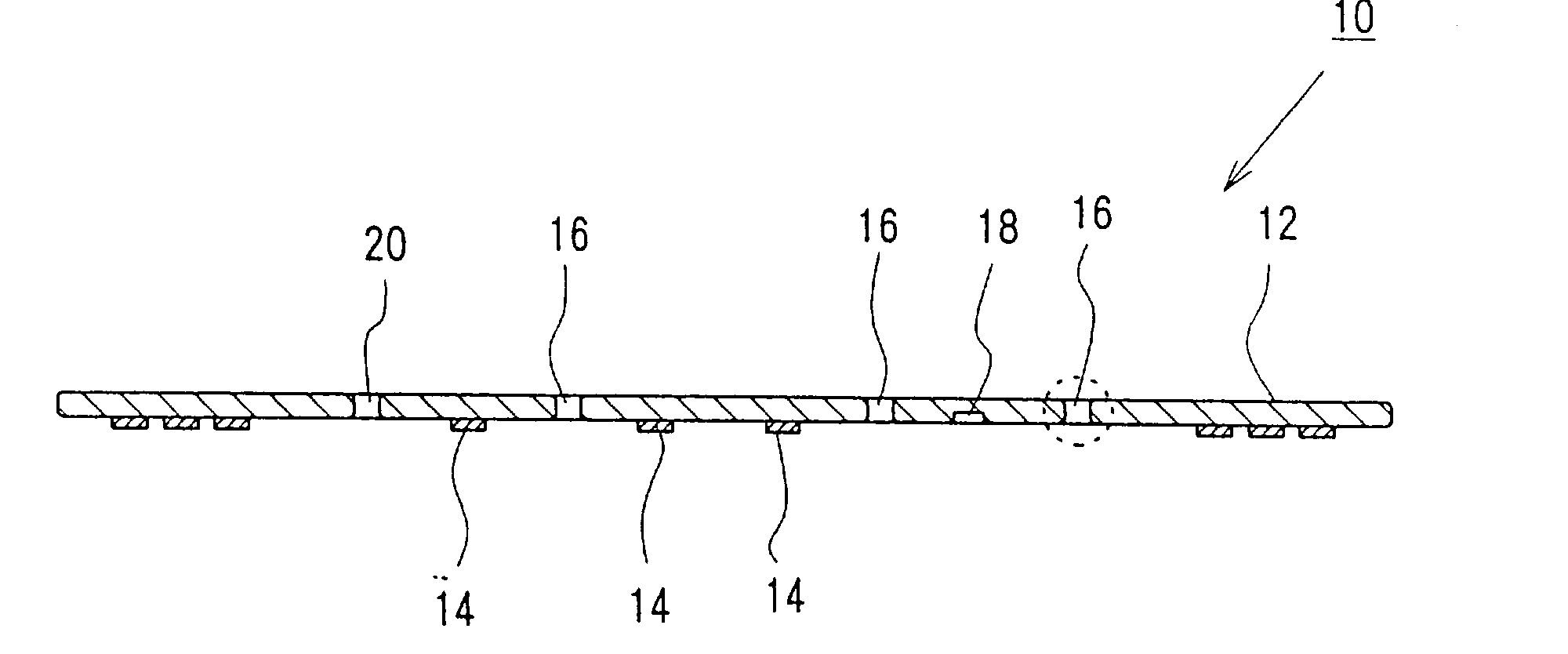
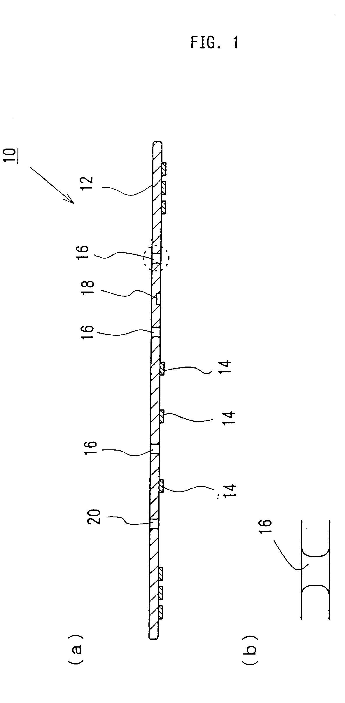
a ceramic heater and heater body technology, applied in the field of ceramic heaters, can solve the problems of uniform cure of resin and thermal shock to the wafer, and achieve the effect of improving uniform temperature distribution

Inactive Publication Date: 2003-07-24
IBIDEN CO LTD
View PDF9 Cites 13 Cited by
  • Summary
  • Abstract
  • Description
  • Claims
  • Application Information

AI Technical Summary

Benefits of technology

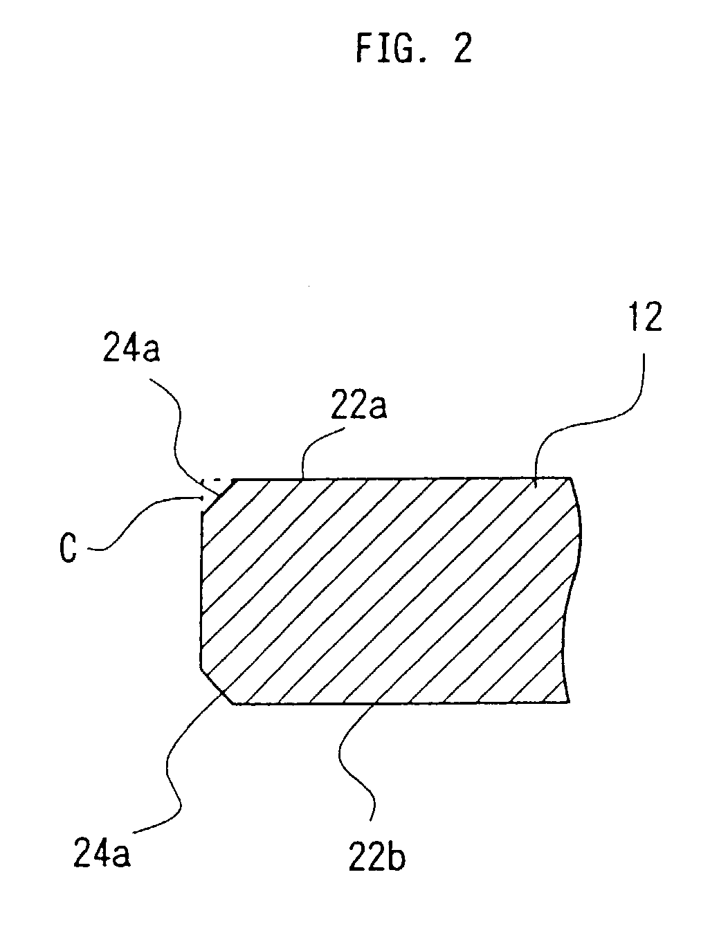
[0012] The present inventors have made earnest studies for overcoming such problems and, as a result, have reached an idea that chamfering for the corner of the ceramic main body has an effect of improving ununiformity in the temperature distribution.

Problems solved by technology

Such low temperature spots may possibly cause thermal shocks to the wafer upon heat-drying treatment.
Further, a resin is sometimes coated on the wafer, which is exposed for development and thermally cured, but there was a problem that the cure of the resin was not uniform.

Method used


Image

  • Ceramic heater
  • Ceramic heater
  • Ceramic heater

Examples


example 1

Manufacture of a Ceramic Heater Having a Heat Generation Body on the Surface of a Ceramic Substrate

[0086] (1) A composition comprising 100 parts by weight of an aluminum nitride powder with an average grain size of 0.6 .mu.m, 4 parts by weight of yttria (average grainze: 0.4 .mu.m), 12 parts by weight of an acrylic binder and alcohol was spray dried to prepare a granular powder.

[0087] (2) Then, the granular powder was placed in a molding die, and molded into a flat plate to obtain a green molding product (green). Drilling was applied to the green molding product by using drills having a diameter of 10 mm and 0.1 mm to form portions as through holes (25 mm diameter) at 18 positions for inserting support pins (lifter pins) of a semiconductor wafer and portions as recesses for burying thermocouples (diameter: 1.1 mm, depth: 2 mm) at 5 positions (A, B, C, F and G in FIG. 13).

[0088] (3) The green molding product after the drilling was hot pressed at 1800.degree. C., under a pressure of 2...

example 2

Manufacture of a Ceramic Heater Having a Heat Generation Body and an Electrostatic Electrode for Electrostatic Chuck

[0101] (1) Paste comprising, in admixture, 100 parts by weight of aluminum nitride (average grainsize: 1.1 .mu.m), 4 parts by weight yttria (average grain size: 0.4 .mu.m), 11.5 parts by weight of an acrylic binder, 0.5 parts by weight of a dispersant and 53% by weight of an alcohol comprising 1-butanol and ethanol was used and molded by a doctor blade method to obtain a green sheet of 0.47 mm thickness.

[0102] (2) Then, after drying the green sheet at 80.degree. C. for five hours, portions as through holes 15 for insertion of semiconductor wafer support pins of 1.8 mm, 3.0 mm and 5.0 mm in diameter and portions as through holes 18 for connection with external terminals were formed by punching.

[0103] (3) 100 parts by weight of tungsten carbide particles of 1 .mu.m average grain size, 3.0 parts by weight of an acrylic binder, 3.5 parts by weight of .alpha.-terpiol solven...

example 3

Manufacture of a Wafer Prober Having a Heater Function

[0112] A waver prober having the heater function was manufactured and it is explained with reference to FIG. 11 and FIG. 12.

[0113] (1) A composition comprising, in admixture, 100 parts by weight of aluminum nitride powder (average grain size: 1.1 .mu.m), 4 parts by weight yttria (average grain size; 0.4 .mu.m), 11.5 parts by weight of an acrylic binder, 0.5 parts by weight of a dispersant and 53% by weight of an alcohol comprising 1-butanol and ethanol described above was formed by a doctor blade to obtain a green sheet 54 of 0.47 mm thickness (refer to FIG. 11(a)).

[0114] (2) After drying the green sheet 54 at 80.degree. C. for five hours, holes for through holes for connecting the heat generation body and the external terminal pins were formed by punching (refer to FIG. 11(a)).

[0115] (3) 100 parts by weight of tungsten carbide particles of 1 .mu.m average grain size, 3.0 parts by weight of an acrylic binder, 3.5 parts by weight ...


PUM

PropertyMeasurementUnit
diameteraaaaaaaaaa
thicknessaaaaaaaaaa
diameteraaaaaaaaaa

Abstract

A ceramic heater capable of reducing temperature uniformity at the periphery of through holes such as insertion holes and vacuum suction holes is provided, which protects wafer against thermal shocks and has improved controllability for temperature control parts such as thermocouples and temperature fuse. Further, a ceramic heater capable of uniform resin curing is provided. A heat generation body is disposed on the surface or inside of a ceramic substrate. Further, corners for the insertion holes, the recesses and the vacuum suction holes of the ceramic substrate are chamfered.

Description

[0001] The present invention relates to a ceramic heater, and more particularly, it relates to a ceramic heater for use in manufacture or inspection processes of semiconductors.[0002] As is well known, semiconductor products are of great importance and semiconductor chips as a typical example thereof are manufactured, for example, by preparing silicon wafers by slicing silicon single crystals to predetermined thickness and then forming various circuits on the silicon wafers.[0003] The various circuits are formed into circuit patterns by sputtering or etching on silicon wafers and, since sputtering or etching is conducted at a high temperature and corrosive gases are sometimes used, they are preferably made of ceramic sintering products.[0004] Such ceramic heaters comprise, as main constituent elements, a ceramic substrate and, a heat generation body disposed substantially over the entire rear face of the substrate, for example, a resistor pattern that generates heat upon current sup...

Claims


Application Information

Patent Timeline
Patent Type & Authority Applications(United States)
IPC IPC(8): H01L21/00
CPCH01L21/67103
Inventor ITO, YASUTAKA
Owner IBIDEN CO LTD
Learn More