Device mounting board and semiconductor apparatus using device mounting board

a technology of device mounting and semiconductor devices, applied in the field of device mounting boards, can solve the problems of reducing yield, reducing position accuracy, and reducing the yield of related art described in the above reference, and achieve excellent reliability and heat-resistant properties

Inactive Publication Date: 2005-10-06
SANYO ELECTRIC CO LTD
View PDF6 Cites 18 Cited by
  • Summary
  • Abstract
  • Description
  • Claims
  • Application Information

AI Technical Summary

Benefits of technology

[0011] In view of the foregoing, an object of the invention is to stably provide a device mounting board which has excellent reliability and heat-resistant properties.
[0012] Another object of the invention is to provide a device mounting board having excellent reliability and heat-resistant properties, in which position accuracy is favorably maintained when the semiconductor device is mounted.
[0014] In the cardo type polymer, because a bulky substituent group obstructs movement of a main chain, the cardo type polymer is excellent for heat-resistant properties and mechanical strength. Because the material containing the cardo type polymer contains the cardo type polymer having high glass transition temperature, the material containing the cardo type polymer can contain other components having high flow properties. Therefore, the material containing the cardo type polymer has characteristics in which moderate flexibility is imparted by heating the material containing the cardo type polymer. When a film containing the cardo type polymer is bonded to form the dielectric film, because little air is involved during the bonding, the dielectric film can stably be manufactured. The manufactured dielectric film is excellent in the heat-resistant properties and the mechanical strength. Further, in the dielectric film, the number of voids is decreased and unevenness is improved. According to the method of present invention, the device mounting board which is excellent in reliability and the heat-resistant properties can stably manufactured.
[0016] In the cardo type polymer, because the bulky substituent group obstructs the movement of the main chain, the cardo type polymer is excellent in the heat-resistant properties and the mechanical strength and the cardo type polymer has the linear expansion coefficient. Therefore, in the heat cycle, the decrease in adhesion properties between dielectric resin layers in the multilayer resin film and the delamination are suppressed in the device mounting board. As a result, the device mounting board which is excellent in reliability and the heat-resistant properties can stably provided.

Problems solved by technology

However, the related art described in the above reference is susceptible to improvement in the following points.
As a result, sometimes a decrease in adhesion properties between dielectric resin layers in the multilayer dielectric film or delamination is caused to reduce yield.
Further, because warp of the device mounting board is caused, sometimes position accuracy is decreased and the yield is reduced when the semiconductor device is connected by a connecting method such as flip chip connection and wire bonding connection.

Method used


Image

  • Device mounting board and semiconductor apparatus using device mounting board
  • Device mounting board and semiconductor apparatus using device mounting board
  • Device mounting board and semiconductor apparatus using device mounting board

Examples


example 1

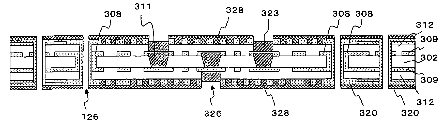
[0222]FIG. 24B is a sectional view showing the device mounting board including the four-layer ISB structure according to Example 1.

[0223] The device mounting board has the structure in which a dielectric resin film 1312 and a photoimageable solder resist film 1328 are sequentially laminated on the upper surface of a base material 1302. The device mounting board also has the structure in which the dielectric resin film 1312 and the photoimageable solder resist film 1328 are sequentially laminated on the lower surface of the base material 1302.

[0224] A through-hole 1327 which pierces through the base material 1302, the dielectric resin film 1312, and the photoimageable solder resist film 1328 is made.

[0225] A part of the piece of wiring made of a copper film 1308, a part of the piece of wiring made of a copper film 1320, a part of a via hole 1311, and the like are embedded in the base material 1302. A part of the piece of the wiring made of the copper film 1308, a part of the piece...

example 2

[0318]FIGS. 26A to 29D are a sectional view schematically showing various semiconductor apparatuses formed by mounting the semiconductor device on the device mounting board described in Example 1.

[0319] There are various modes in the semiconductor apparatus formed by mounting the semiconductor device on the device mounting board described in Example 1. For example, there is the mode in which the semiconductor device is mounted on the device mounting board by the flip chip connection or the wire bonding connection. There is the mode the semiconductor device is mounted on the device mounting board by taking the face up structure or the face down structure. There is the mode in which the semiconductor element is mounted on one side or both sides of the device mounting board. There is the mode in which these various modes are combined.

[0320] Specifically, as shown in FIG. 26A, a semiconductor device 1500 such as LSI can be mounted on a device mounting board 1400 of the Example 1 in th...


PUM


Abstract

The device mounting board according to the first embodiment has the structure in which an dielectric resin film and a photoimageable solder resist film are sequentially laminated on an upper surface of a base material. The device mounting board also has the structure in which the dielectric resin film and the photoimageable solder resist film are sequentially laminated on a lower surface of the base material. The photoimageable solder resist film contains the cardo type polymer.

Description

BACKGROUND OF THE INVENTION [0001] 1. Field of the Invention [0002] The present invention relates to a device mounting board, a manufacturing method thereof, and a semiconductor apparatus using the device mounting board. [0003] 2. Description of the Related Art [0004] Recently, multifunction and high performance of portable electronic devices such as a cellular phone, PDA, DVC, and DSC are accelerated, so that miniaturization and weight reduction are necessary in order that such electronic devices are accepted in the market. A highly integrated system-LSI is required in order to realize the miniaturization and the weight reduction. On the other hand, the ease-to-use and convenient electronic devices are demanded, and the multifunction and the high performance are demanded for LSIs used for the electronic devices. Therefore, while the number of I / Os are increased as an LSI chip is integrated, and the miniaturization of a package itself is also demanded. In order to achieve compatibil...

Claims


Application Information

Patent Timeline
Patent Type & Authority Applications(United States)
IPC IPC(8): H01L21/00H01L21/48H01L23/12H01L23/498H01L23/58H05K1/03H05K3/28H05K3/46
CPCH01L21/4857H01L23/49894H01L2224/45144H01L2924/01019H01L24/49H01L24/48H01L2224/16225H01L2224/48227H01L2224/49171H01L2924/01046H01L2924/01078H01L2924/01079H01L2924/15311H01L2924/19041H01L2924/19105H01L2924/3025H05K3/287H05K3/4602H01L2924/00H01L2924/12042H01L2924/181H01L2224/05554H01L2924/00014H01L24/45H01L2924/00012H01L2224/45015H01L2924/207
Inventor USUI, RYOSUKENAKAMURA, TAKESHIMIZUHARA, HIDEKI
Owner SANYO ELECTRIC CO LTD
Why Eureka
Try Eureka