
Electrostatic chuck for holding wafer

a technology of electrostatic chuck and wafer, which is applied in electrostatic holding devices, emergency protective arrangement details, electrical devices, etc., can solve the problems of deterioration of wafer qualities, variation of etching rate, and inability to uniformly etch the overall surface of the wafer

Inactive Publication Date: 2003-08-28
KYOCERA CORP
View PDF7 Cites 57 Cited by
  • Summary
  • Abstract
  • Description
  • Claims
  • Application Information

AI Technical Summary

Problems solved by technology

In deposition apparatuses, reactive gas used in the process of deposition often heats a wafer on a chuck and causes the wafer to have a non-uniform temperature distribution on its surface, thereby in some cases, resulting in a deterioration in wafer qualities.
Also, wafers are heated by plasma gaseous etchant in etching apparatuses, or with ultraviolet or visible light illuminated in patterned photo-projection etching so that a temperature distribution over the wafer surface is made non-uniform, thereby causing variations in etching rate to an extent that the overall surface of the wafer cannot be uniformly etched.
A problem of how to implement a uniform temperature distribution over the wafer surface has been held without resolution.
However, the electrostatic chuck according to Japanese Patent Publication No. 07-153825 attractively holds the wafer W via the top surfaces of the many protrusions 24 together with an outer-peripheral portion 25 so that an wafer W with a flection or warp cannot perfectly attracted on the chuck while such a warped wafer is only partly attracted thereon, resulting in lack of attraction force to the wafer, thereby causing, for example, migrating of the wafer on the chuck, or in some cases, falling of the wafer from the chuck stage.
The resulting gap allows a leakage of the heat-conductive gas, thereby reducing a vacuum during processing and adversely affecting dimensional of fabricated films thereon
Consequently, since the flatness of the mounting surface 54 is reduced at the time of various water processes, processing accuracy for the wafer W cannot be enhanced.
There arises a problem that thin ceramic plates having a thickness not greater than 5.0 mm are apt to be warped.

Method used


Image

  • Electrostatic chuck for holding wafer
  • Electrostatic chuck for holding wafer
  • Electrostatic chuck for holding wafer

Examples


embodiment 1

[0050]

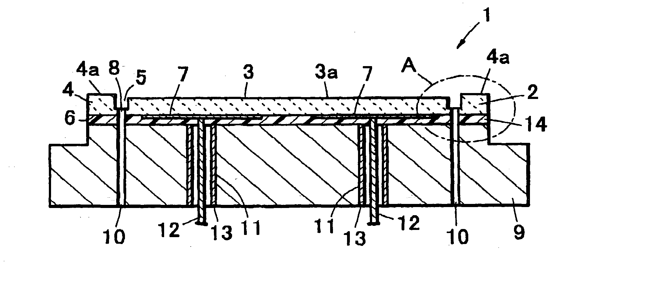
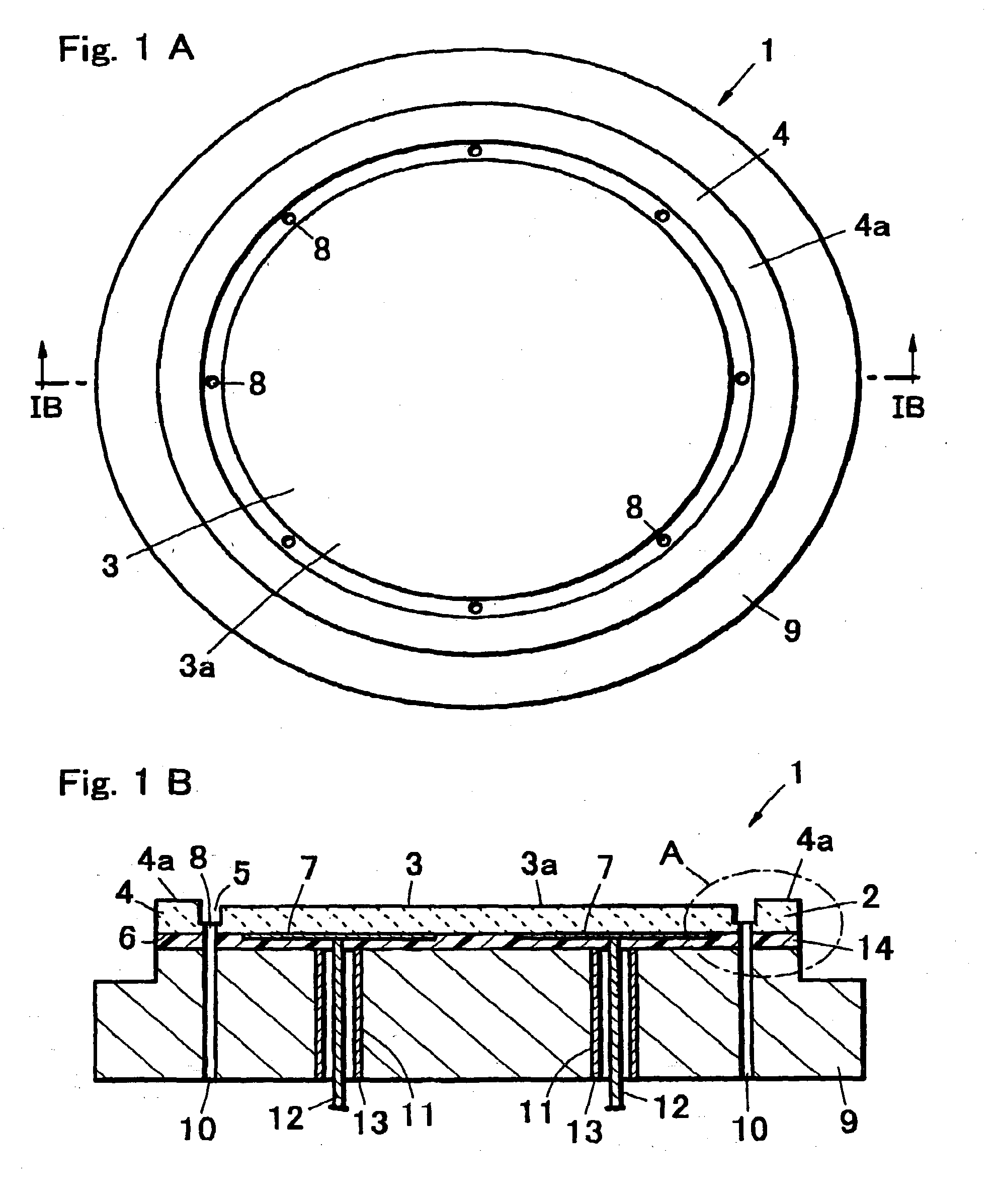
[0051] An electrostatic chuck 1 of this embodiment according to the present invention include a ceramic plate having a mounting surface on one main surface thereof, and a attractive electrode buried within the ceramic plate or attached on the other main surface, a recess portion 3 shaped circular as viewed in a plan view is formed on the one main surface except fox an outer peripheral portion 4 of a disc-shaped ceramic plate 2 having the substantially same size as a wafer. A top face of the outer peripheral portion 4 is used as a second holding surface 4a.

[0052] In this embodiment, a gas groove 5 is provided on a peripheral portion on a bottom surface of the recess portion 3 (which hereinbelow will be referred to as a "recess-portion bottom surface") that is surrounded by the gas groove 5 is used as a first holding surface 3a. A pair of semicircular electrostatic: attraction electrodes 7 are formed on an other main surface 6 of the ceramic plate 2 provided below the recess-por...

first example

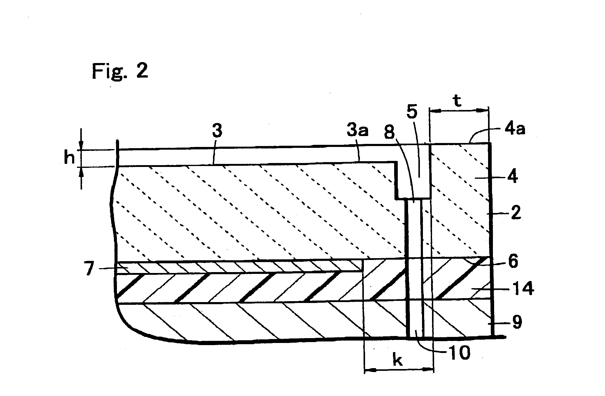
[0088] Electrostatic chucks 1 shown in FIG. 1 were manufactured and experiments were carried out to investigate the temperature variation, the amount of leakage of a heat-conductive gas, and the dechucking sensitivity in the surface of the wafer by providing recess portions having different depths h.

[0089] In the experiments, fox each of the electrostatic chucks 1, a disc-shaped ceramic plates 2 was prepared of a sinter of aluminum nitride with a diameter of 200 mm and a thickness of 1 mm. A nickel film for an electrostatic electrode 7 was applied on the other main surface of the ceramic plate 2 by a plating technique, subsequently, unnecessary portions were etched to remove, and electrostatic attraction electrodes 7 composed of a pair of semicircular nickel films was prepared to be of a circular shape.

[0090] Power feeders 12 were adhered to each electrostatic attraction electrodes 7 via a conductive adhesive, and thereafter an aluminum base member 9 was adhered to the other main su...

second example

[0100] Experiments were carried out to investigate the wafer-surface temperature variation, the amount of leakage of the heat-conductive gas, and the dechucking sensitivity. The experiments were carried out. in the same conditions as those in the first example except that the depth h of the recess portion 3 was fixed at 5 .mu.m, and the waviness of the top face of the outer peripheral portion 4 was changed. The results are shown in Table 2.

2TABLE 2 HELIUM WAFER DECHUCKING LEAKAGE TEMPERATURE SENSITIVE DEPTH WAVINESS DISTANCE AMOUNT VARIATIONS TIME NO. (.mu.m) (.mu.m) (mm) (SCCM) .DELTA.T(.degree. C.) (sec) 6 5 0.5 5 2.4 4.5 13.5 7 5 1 5 2.8 4.8 7.6 8 5 3 5 3.5 4.9 5.3 9 5 5 5 12.7 11.8 4.5

[0101] As can be seen in Table 2, in test sample No. 6 in which the waviness of the top face of the outer peripheral portion 4 is 0.5 .mu.m, the dechucking sensitive time was as long as 13.5 seconds. This is considered to have occurred for the reason that since the waviness of the outer peripheral ...


PUM


Abstract

An electrostatic chuck for holding a wafer includes a ceramic plate of which one main surface is formed to work as a mounting surface for mounting the wafer, and electrostatic attraction electrodes formed on a lower surface of the ceramic plate or in the ceramic plate. A recess portion having a depth in a range of from 3 to 10 mum is formed on one main surface of the ceramic plate excluding an outer peripheral portion thereof. The waviness of a top face of the outer peripheral portion is set to 1 to 3 mum, a gas groove is provided to a peripheral portion of a bottom surface of the recess-portion bottom surface, and electrostatic attraction electrodes are disposed in the ceramic plate disposed below the bottom surface of the convex portion. In the electrostatic chuck thus constructed, even a wafer having a deformation such as a warped portion can be firmly attracted, a uniform temperature distribution over a wafer surface can be implemented, leakage of a heat-conductive gas can be suppressed, and moreover, high wafer-dechucking sensitivity can be exhibited.

Description

[0001] 1. Field of the Invention[0002] The invention relates to an electrostatic chuck for attractively holding a wafer such as a semiconductor wafer thereon.[0003] 2. Prior Art[0004] Conventionally, electrostatic chucks are used for accurately holding and positioning a semiconductor wafer (which hereinbelow will shortly be referred to as a "wafer") thereon, primarily in a semiconductor manufacturing systems which include various deposition apparatuses (for example, for PVD, CVD, or plasma CVD processes) and etching apparatuses (for example, for plasma etching or optical etching).[0005] Processes in many semiconductor-manufacturing apparatuses are often performed under a vacuum. In deposition apparatuses, reactive gas used in the process of deposition often heats a wafer on a chuck and causes the wafer to have a non-uniform temperature distribution on its surface, thereby in some cases, resulting in a deterioration in wafer qualities.[0006] Also, wafers are heated by plasma gaseous ...

Claims


Application Information

Patent Timeline
IPC IPC(8): H01L21/00H01L21/683H02N13/00
CPCH01L21/6831H01L21/67109
Inventor MIGITA, YASUSHI
Owner KYOCERA CORP
Learn More