
Eureka
For R&D, Eureka makes reading and utilizing patents & technical documents easy.
Eureka AIR
Designed for self-driven R&D workflows. Generate viable solutions, solve complex R&D challenges, empower your innovation with AI.

Eureka Materials
Designed for material experts only. Revolutionize your material R&D, from search, analyze, to developing new materials.

TechResearch
Generate reliable direction feasibility study reports for your R&D in just a few steps.

TechSeek
Discover and master advanced knowledge NOW. Basics, ideas, possibilities, all at once.

TechMind
As an expert in R&D Theories, TechMind can generates customized viable solutions instantly.

TechRisk
Analyze your overall solution with one click, know your potential R&D risks in advance.

TechMonitor
Get weekly tech updates, stay abreast of the latest tech innovations and key insights.
Optical module
- Summary
- Abstract
- Description
- Claims
- Application Information
AI Technical Summary
Problems solved by technology
Method used
Image

Examples
first embodiment
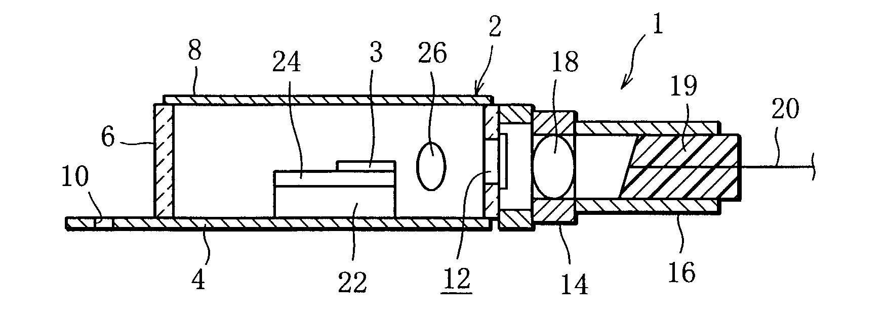
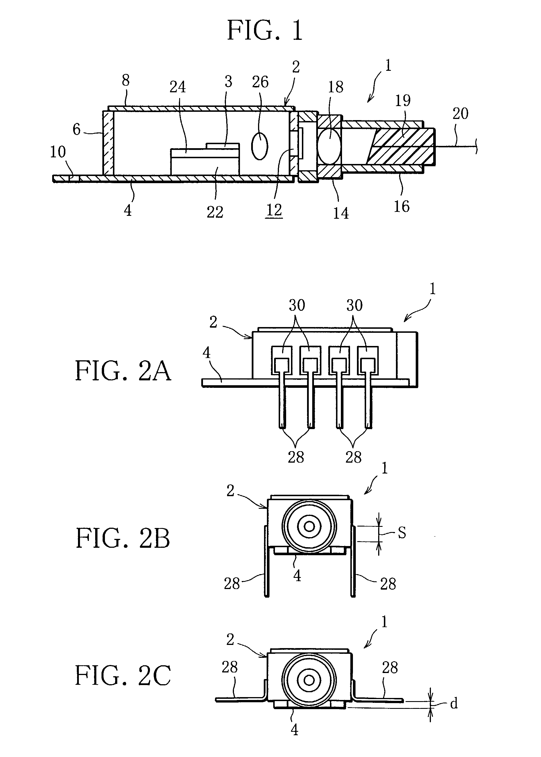
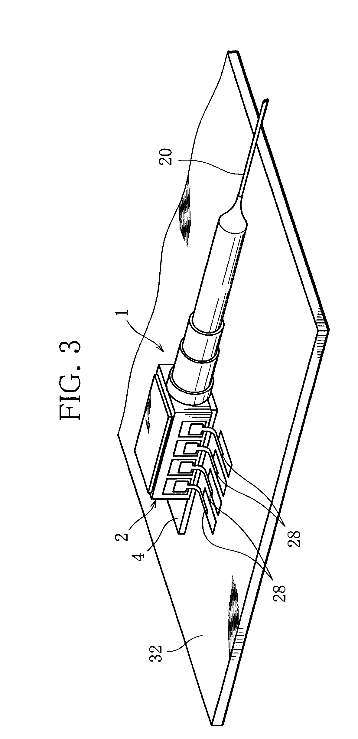
[0033] FIGS. 2A to 2C specifically show the lead pin 28 in the semiconductor laser module 1 according to the Four pairs of the lead pins 28 are provided to both the side surfaces of the package 2, and four lead pins 28 form one line along each side surface. Thus, the lead pins 28 form two lines each on the respective side surfaces of the package 2, and all of the lead pins 28 extend downward from the side surface. For that, the package 2 is a so-called DIL package. Note that, in the illustrated example, four pairs of the lead pins 28, more specifically, the total of eight pins are provided. However, the number of the lead pins 28 is not limited to this.
[0034] Four plating patterns 30 for use in the soldering are formed on each side surface of the package 2. The arrangement of these plating patterns 30 is determined depending on the number of the lead pins 28 to be attached (FIG. 2A). The base end portion of the lead pin 28 is widened to form a square-shaped pad providing a predeter...
second embodiment
[0049] FIGS. 8A to 8C show the semiconductor laser module according to the In this embodiment, chamfer portions 36 are provided on both the side surfaces of the package 2, that is, on the lower portion of the side wall 6. These chamfer portions 36 are formed by obliquely cutting the corner portions between the bottom surface of the package 2 and the fixing region S of the lead pins 28. As a result, the plating patterns 30 are formed on both the side surfaces of the package 2 above the chamfer portions 36. Moreover, both the edge portions of the bottom plate 4 almost correspond to the borders of the chamfer portions 36 (FIG. 8B).
[0050] As shown in FIGS. 8B and 8C, the chamfer portion 36 forms a space between the bottom and side surfaces of the package 2 and the fixing region S. Therefore, the access to the lead pin 28 is facilitated owing to the space, and the process for bending the lead pin 28 is further facilitated.
[0051] FIGS. 9 and 10 show an example of the case where the semic...
third embodiment
[0053] As shown in FIGS. 11B and 11C, also in the third embodiment, the chamfer portion 36 forms a space between the bottom and side surfaces of the package 2 and the fixing region S, thereby the process for laterally bending the lead pin 28 is facilitated.
[0054] Furthermore, FIG. 12 shows the semiconductor laser module 1 according to the fourth embodiment. In this embodiment, instead of the chamfer portions 36 described in the third embodiment, notched grooves 38 are formed in each of the corner portions. The notched grooves 38 are formed by cutting the corner portions on both the sides along the longitudinal direction. By the notched groove 38, the corner portion between the fixing region S of the lead pin 28 and the bottom surface are cut off. As a result, the plating patterns 30 are formed on both the side surfaces of the package 2 above the notched grooves 38.
PUM
 Abstract
Description
Claims
Application Information
 - R&D Engineer
- R&D Manager
- IP Professional
- Industry Leading Data Capabilities
- Powerful AI technology
- Patent DNA Extraction
Browse by: Latest US Patents, China's latest patents, Technical Efficacy Thesaurus, Application Domain, Technology Topic, Popular Technical Reports.
© 2024 PatSnap. All rights reserved.Legal|Privacy policy|Modern Slavery Act Transparency Statement|Sitemap|About US| Contact US: help@patsnap.com