Semiconductor device including low-resistance wires electrically connected to impurity layers

a technology of impurity layer and resistance wire, which is applied in the direction of semiconductor devices, semiconductor/solid-state device details, electrical apparatus, etc., can solve the problems of difficulty in flow of source-drain current, inability to meet the demand for shrinkage of semiconductor devices, and ineffective high-speed operations

Inactive Publication Date: 2003-10-09
RENESAS TECH CORP
View PDF4 Cites 14 Cited by
  • Summary
  • Abstract
  • Description
  • Claims
  • Application Information

AI Technical Summary

Problems solved by technology

Therefore, a demand for shrinkage of a semiconductor device cannot be met.
As a result, high speed operations are less effecti...

Method used


Image

  • Semiconductor device including low-resistance wires electrically connected to impurity layers
  • Semiconductor device including low-resistance wires electrically connected to impurity layers
  • Semiconductor device including low-resistance wires electrically connected to impurity layers

Examples


Embodiment Construction

>

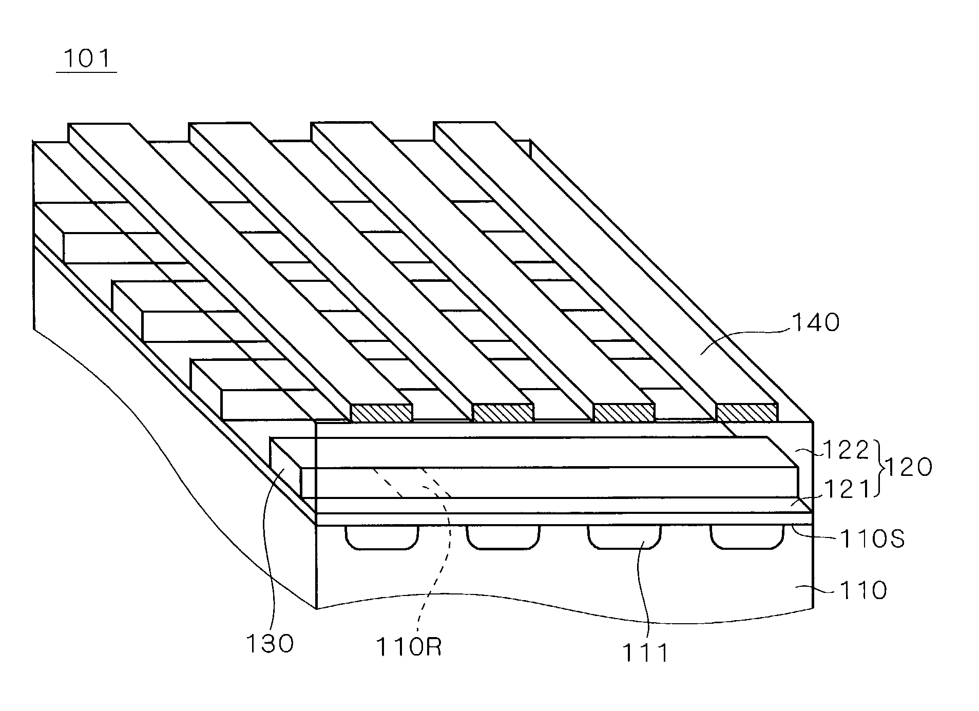
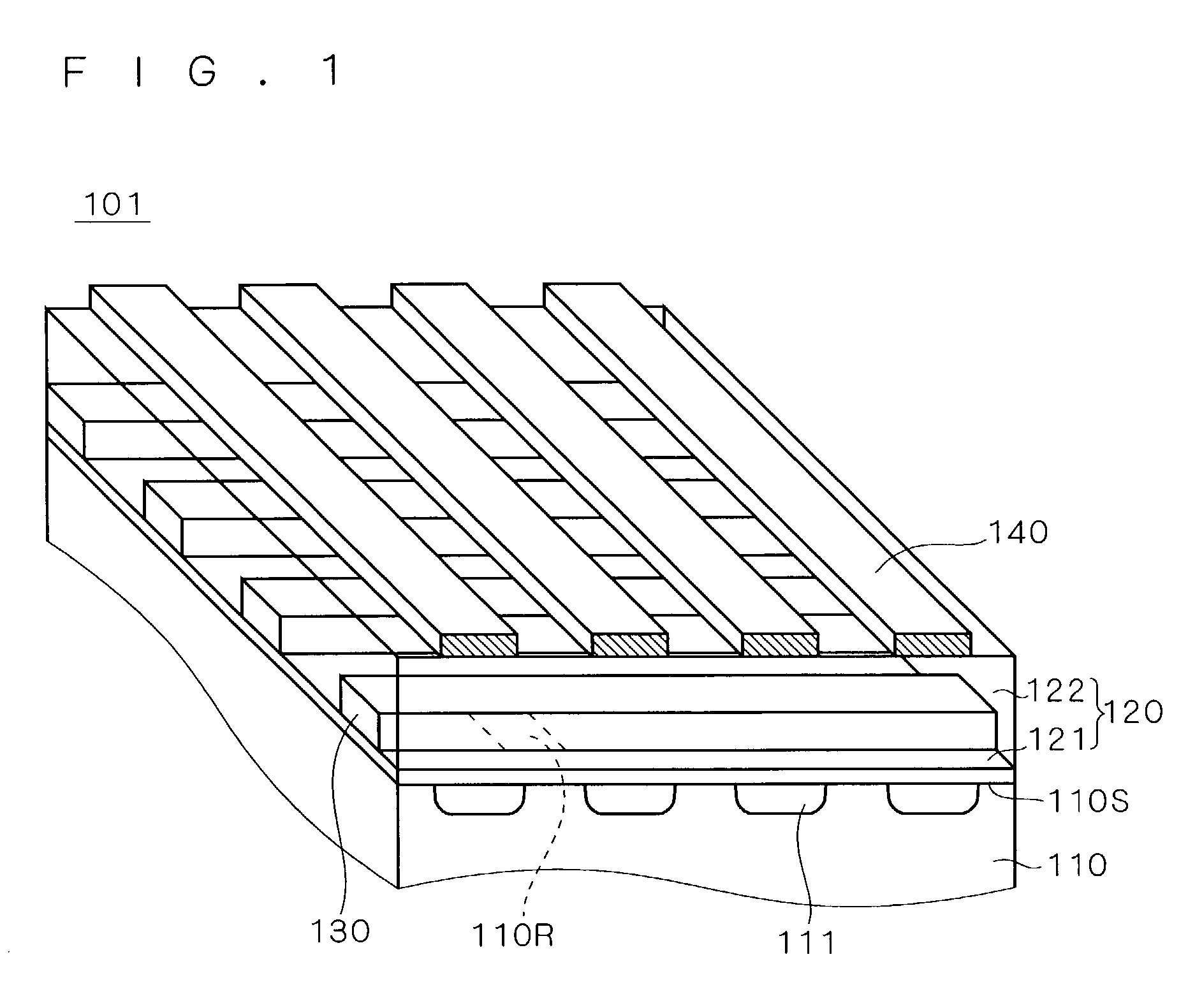
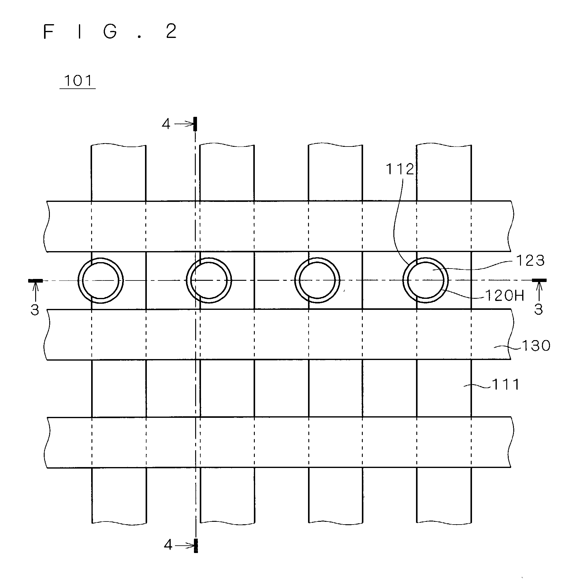
[0111] The unit cell in the foregoing semiconductor device 101 may be a diode formed by providing an electrical short circuit between the drain and gate. The operations of the unit cell having a diode structure thus formed will be described with reference to FIGS. 29 and 30.

[0112] First, as given in FIG. 29, a short circuit is provided between the drain and gate and a forward bias voltage is applied across the drain and source. The unit cell is thereby brought into the same condition as in the unit cell given in FIG. 12 including the depletion layer 10a. Due to the formation of the depletion layer 10a, the induced in-channel charges 9a disappear.

[0113] As the gate and drain are short circuited, an N-type channel is formed in the channel-forming region of the semiconductor substrate 110, allowing a drain-source current to flow. The in-channel charges 9a are cancelled out by the depletion layer 10a and therefore, they cause no effect on the formation of the N-type channel.

[0114] On t...


PUM


Abstract

A plurality of N-type first impurity layers (111) are provided that form stripes in a main surface (110S) of a P-type semiconductor substrate (110). At least one N-type second impurity layer (112) overlaps (or touches) one of the first impurity layers (111). A plurality of gate electrodes are provided on a gate insulating film (121). A plurality of gate electrodes form stripes crossing the first impurity layers (111). A plurality of low-resistance wires (140) are provided on an interlayer insulating film (122). The plurality of low-resistance wires (140) form stripes extending in the same direction as that of the first impurity layers (111). An end (123T2) of each contact plug (123) is entirely in contact with the second impurity layer 112, and does not touch a P-type region of the semiconductor substrate (110).

Description

[0001] 1. Field of the Invention[0002] The present invention relates to a semiconductor device. More particularly, it relates to a technique for ensuring electrical connection between a contact plug and an impurity layer even on the occurrence of misalignment of a contact hole.[0003] 2. Description of the Background Art[0004] FIG. 31 is a perspective view illustrating a semiconductor device or semiconductor memory device 901 according to a first background art. The semiconductor device 901 is a semiconductor memory device including a plurality of transistors each having a so-called MONOS (metal-oxide-nitride-oxide-semiconductor) structure. This type of semiconductor memory device is disclosed in U.S. Pat. No. 5,768,192, for example.[0005] The semiconductor device 901 has a plurality of N-type impurity layers 911 forming stripes in a main surface 910S of a P-type semiconductor substrate 910. An ONO film 921 serving as a gate insulating film is arranged on the main surface 910S. The O...

Claims


Application Information

Patent Timeline
IPC IPC(8): H01L21/336H01L21/28H01L21/768H01L21/8246H01L21/8247H01L23/485H01L23/522H01L27/115H01L29/772H01L29/788H01L29/792
CPCH01L23/485H01L27/115H01L27/11568H01L29/66833H01L2924/13091H01L2224/48095H01L2224/73265H01L29/792H01L2924/00014H10B69/00H10B43/30H01L2924/00H01L29/772
Inventor YAMASHITA, TOMOHIRO
Owner RENESAS TECH CORP
Why Eureka
Try Eureka