Multilayer printed circuit board and method of manufacturing multilayer printed circuit board

Inactive Publication Date: 2003-10-23
SONY CORP
View PDF10 Cites 33 Cited by
  • Summary
  • Abstract
  • Description
  • Claims
  • Application Information

AI Technical Summary

Benefits of technology

[0009] More specifically, the present invention provides a multilayer printed circuit board which can prevent flowage of a conductive cement using at a part where the interlayer connection is established so as to prevent a metal migration from being generated when jointing layers, and providing a method of manufacturing the multilayer printed circuit board.
[0012] According to the multilayer printed circuit board of the present invention, the interlayer connection is established by engaging the conductive bumps formed integrally on the conductive patterns with the connection holes formed on the substrates. The multilayer printed circuit board is integrated by laminating the substrates where the bumps are engaged with the connection holes and heat-pressing them together. Therefore, the substrates can be laminated without displacement. In addition, the bumps and the lands are connected each other through the conductive cement in the connection holes, it can prevent spreading of the conductive cement and generating of metal migration because a single heat-pressing is enough to be performed. In addition, since the bumps and the lands are connected through the conductive cement, the interlayer connection is surely established.

Problems solved by technology

However, the build-up process has disadvantage such that if any failure occurs with a layer, all layers will be defective, thus productivity decreases.
Further, in the build-up process, it tends to produce a defective due to cracking in an insulating layer because a heat compression is repeated for laminating substrates.
However, when the re-flow process is performed to the substrate for mounting electronic components, the tin-lead solder melts again and expands due to its low melting point, hence there may be possibly generated wire breaking.

Method used


Image

  • Multilayer printed circuit board and method of manufacturing multilayer printed circuit board
  • Multilayer printed circuit board and method of manufacturing multilayer printed circuit board
  • Multilayer printed circuit board and method of manufacturing multilayer printed circuit board

Examples


Embodiment Construction

)

[0026] Hereinafter, a multilayer printed circuit board, to which the present invention is applied, will be described in detail with reference to the accompanying drawings.

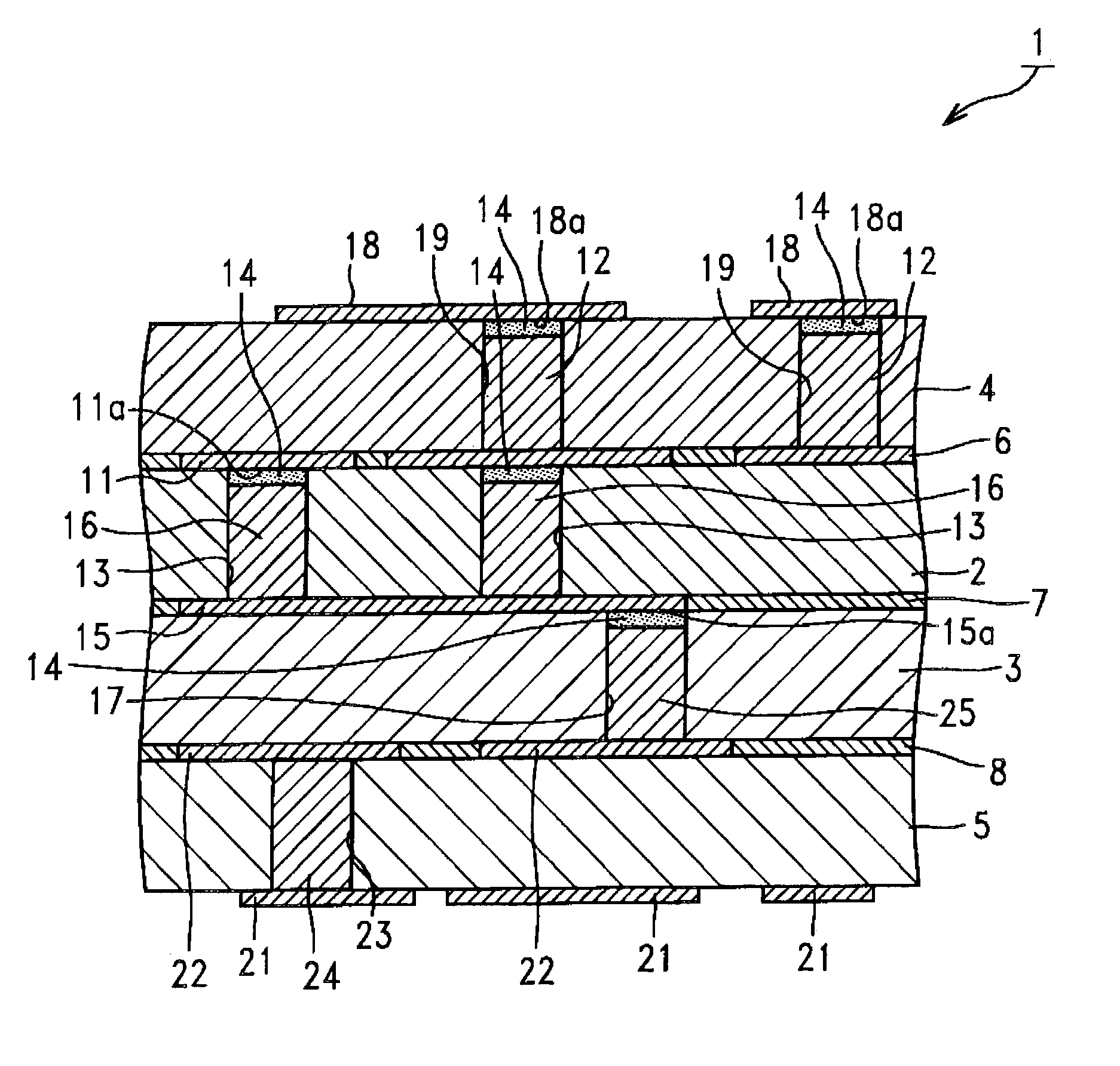
[0027] As shown in FIG. 1, a multilayer printed circuit board 1 to which the present invention is applied has inner layer substrates 2, 3 and outer layer substrates 4, 5. The substrates 2, 3, 4, 5 are laminated having each of insulating layers 6, 7, 8 therebetween, respectively, and are integrated together. The insulating layers 6, 7, 8 are used for adhering the adjacent substrates 2, 3, 4, 5. Here, it is preferred to use an adhesive agent, which serves as the insulating layers 6, 7, 8, having the same or similar plasticity as a resin used for the inner layer substrates 2, 3 and the outer layer substrates 4, 5. For example, when using glass fiber impregnated with a thermosetting epoxy resin for the substrates 2, 3, 4, 5, an epoxy adhesive agent being a thermosetting adhesive agent is used for the insulating layers...


PUM

PropertyMeasurementUnit
Diameteraaaaaaaaaa
Electrical conductoraaaaaaaaaa
Adhesivityaaaaaaaaaa

Abstract

A multilayer printed circuit board which can surely establish interlayer connection with low resistance. The multilayer printed circuit board comprises: a first substrate having a conductive pattern on one face and a non-penetration connection hole on the other face, for exposing the conductive pattern to outside; a second substrate having a conductive pattern formed on a face opposed to the other face of first substrate and a conductive bump on the conductive pattern integrally. The first substrate and the second substrate are integrated by engaging the bump of the second substrate with the connection hole of the first substrate and by intervening a conductive cement between the bumps and the conductive pattern exposed to outside from the connection holes.

Description

[0001] The present document is based on Japanese Priority Document JP2002-119657, filed in the Japanese Patent Office on Apr. 22, 2002, the entire contents of which being incorporated herein by reference.[0002] 1. Field of the Invention[0003] The present invention relates to a multilayer printed circuit board in which a plurality of conductive layers are electrically connected each other through bumps, and to a method for manufacturing the multilayer printed circuit board.[0004] 2. Description of the Related Art[0005] As a method of manufacturing a multilayer printed circuit board, there is a method so-called build-up process which is carried out as follows. At first, forming a conductive pattern on an inner layer substrate, then forming an insulating layer on the inner layer substrate formed the conductive pattern, and then further forming a conductive pattern on the insulating layer. Repeating this process, a plurality of conductive layers are formed. However, the build-up process...

Claims


Application Information

Patent Timeline
IPC IPC(8): H05K3/06H05K3/32H05K3/38H05K3/42H05K3/46
CPCH05K3/064Y10T29/49165H05K3/386H05K3/423H05K3/462H05K3/4623H05K3/4647H05K3/4658H05K2201/0195H05K2201/0355H05K2201/0394H05K2203/0733H05K2203/135Y10T29/49155H05K3/321
Inventor FUJII, KENTAROWATANABE, YOSHIOTAKEBE, TORU
Owner SONY CORP
Why Eureka
Try Eureka