Reflection electrode, preparation method thereof and LED chip

A technology of LED chips and reflective electrodes, applied in circuits, electrical components, semiconductor devices, etc., can solve problems such as poor adhesion between silver films and substrates, and achieve the effects of improving electrical properties, efficient bonding, and preventing reflectivity from falling

Pending Publication Date: 2022-03-25
HUAIAN AUCKSUN OPTOELECTRONICS TECHNOLOGY CO LTD
View PDF8 Cites 1 Cited by
  • Summary
  • Abstract
  • Description
  • Claims
  • Application Information

AI Technical Summary

Problems solved by technology

[0004] An object of the present invention is to provide a reflective electrode to solve the technical problem of poor adhesion between the silver film and the substrate caused by electron beam evaporation film formation in the prior art

Method used


Image

  • Reflection electrode, preparation method thereof and LED chip
  • Reflection electrode, preparation method thereof and LED chip
  • Reflection electrode, preparation method thereof and LED chip

Examples


preparation example Construction

[0096] Preferably, the method for preparing the reflective electrode further includes: vapor-depositing a metal protective layer on the metal covering layer.

[0097] More preferably, the evaporation rate of the metal protection layer is 1A / S˜4A / S, more preferably 1A / S˜3A / S.

[0098] In one embodiment, the evaporation rate of the metal protection layer is specifically 2A / S, 3A / S, 4A / S, etc., and other values ​​within the above range can also be selected, which is not limited here.

[0099] According to another aspect of the present invention, the present invention also relates to an LED chip, comprising the above-mentioned reflective electrode.

[0100] The reflective electrode of the present invention can be applied to LED chips, including front-mount, flip-chip or vertical structures. For example, you can attach Figure 6 The Ag mirror structure shown and the attached Figure 7 ODR structure shown.

[0101]Wherein, the Ag reflector structure includes: sapphire substrate,...

Embodiment 1

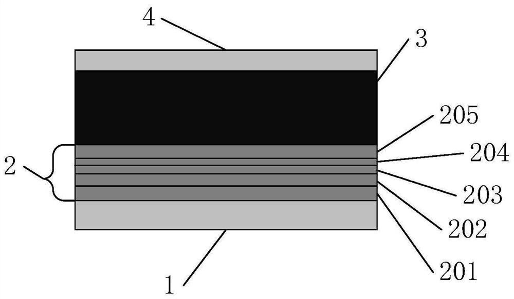
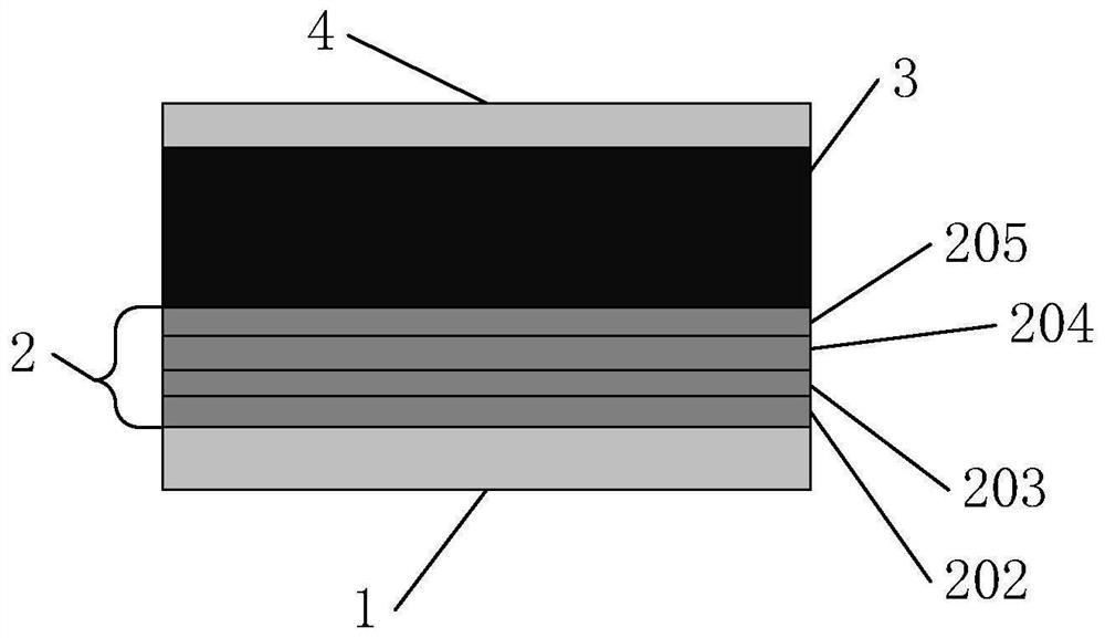
[0110] A reflective electrode, comprising a metal reflective layer 1, a stacked metal barrier layer 2, a metal covering layer 3 and a metal protective layer 4 arranged in sequence;

[0111] The metal reflective layer 1 is an Ag layer with a thickness of 1000A and a Mohs hardness of 2.5;

[0112] The stacked metal barrier layer 2 is a first Ti layer 201, a first Ni layer 202, a first Pt layer 203, a second Ni layer 204 and a second Pt layer 205 arranged in sequence, wherein the first Ti layer 201 Connected with the metal reflective layer 1, the first Ti layer 201 (Mohs hardness is 6), the first Ni layer 202 (Mohs hardness is 4), the first Pt layer 203 (Mohs hardness is 4.5), the second Ni layer The thicknesses of 204 (Mohs hardness is 4) and the second Pt layer 205 (Mohs hardness is 4.5) are 1000A, 600A, 600A, 600A, 600A;

[0113] The metal covering layer 3 is an Au layer with a thickness of 7000A and a Mohs hardness of 2.5;

[0114] The metal protective layer 4 is a Ti layer...

Embodiment 2

[0123] A reflective electrode, except that the laminated metal barrier layer 2 includes a first Ni layer 202, a first Pt layer 203, a second Ni layer 204, and a second Pt layer 205 that are sequentially connected, and the first Ni layer 202 is connected with the metal reflective electrode. The layers 1 are connected, the thicknesses of the first Ni layer 202 , the first Pt layer 203 , the second Ni layer 204 and the second Pt layer 205 are respectively 800 Å, and other conditions are the same as in the first embodiment.

[0124] The preparation method of the reflective electrode in this embodiment is the same as that in Embodiment 1.


PUM

PropertyMeasurementUnit
Mohs hardnessaaaaaaaaaa
hardnessaaaaaaaaaa

Abstract

The invention relates to the technical field of semiconductor devices, in particular to a reflecting electrode, a preparation method of the reflecting electrode and an LED chip. The reflecting electrode comprises a metal reflecting layer, a laminated metal barrier layer and a metal covering layer which are connected in sequence, the metal reflecting layer comprises an Ag layer; the laminated metal barrier layer comprises at least two of a Ti layer, a Ni layer, a Pt layer and a Cr layer; the metal covering layer comprises at least one of an Au layer, a Cu layer, an Al layer and a Zn layer. Through cooperation of the metal reflecting layer, the laminated metal barrier layer and the metal covering layer, efficient bonding between the metal reflecting layer and the substrate is achieved, meanwhile, the stability of the metal reflecting layer can be guaranteed, metal migration of the metal reflecting layer is prevented, and the problem of tilting caused by tensile stress due to different Mohs hardness can be solved.

Description

technical field [0001] The invention relates to the technical field of semiconductor devices, in particular to a reflective electrode, a preparation method thereof, and an LED chip. Background technique [0002] The existing silver-plated thin films mainly adopt two methods of sputtering and electron beam evaporation. Among them, the sputtering method has the following defects: the energy of the sputtering process is relatively large, which will cause damage to the substrate and easily cause crystal defects, which will cause yield problems in the later chip manufacturing process; the number of sputtering equipment target sources is relatively limited. The design of metal laminated electrodes also requires evaporation; the high price of sputtering equipment is not conducive to cost control. In the existing evaporation technology for silver plating, the kinetic energy of silver atoms is small during film formation, and the binding energy of film formation on the substrate is ...

Claims


Application Information

Patent Timeline
Patent Type & Authority Applications(China)
IPC IPC(8): H01L33/40
CPCH01L33/405
Inventor 李明
Owner HUAIAN AUCKSUN OPTOELECTRONICS TECHNOLOGY CO LTD
Why Eureka
Try Eureka