Thermoelectric module package

a technology of thermoelectric modules and modules, applied in the field of semiconductor lasers, lasers, heat exchange devices, etc., can solve the problems of increasing the overall manufacturing cost, increasing the manufacturing cost of packages, and reducing the yield of manufactur

Inactive Publication Date: 2003-11-20
YAMAHA CORP
View PDF2 Cites 27 Cited by
  • Summary
  • Abstract
  • Description
  • Claims
  • Application Information

AI Technical Summary

Problems solved by technology

The aforementioned optical semiconductor module has problems in that it requires a relatively large number of parts, each of which should be specifically processed, and expensive materials are therefore required, increasing the overall manufacturing cost thereof.
In addition, numerous parts are assembled together by respective brazing at high temperature, which results in a reduction of yield in manufacture.
Furthermore, due to troublesome operations performed in high-temperature conditions, it is necessary to use a specific assembling machine that is expensive, which inevitably raises the manufacturing cost of packages.
In addition, there is another problem in that complicated wiring is required in an optical semiconductor module using ceramic field through members.
This results in a relatively low heat radiation efficiency, and therefore it is difficult to rapidly radiate heat to the outside.

Method used


Image

  • Thermoelectric module package
  • Thermoelectric module package
  • Thermoelectric module package

Examples


first embodiment

[0082] The first embodiment can be modified in various ways, examples of which will be described below.

first modification

(a) First Modification

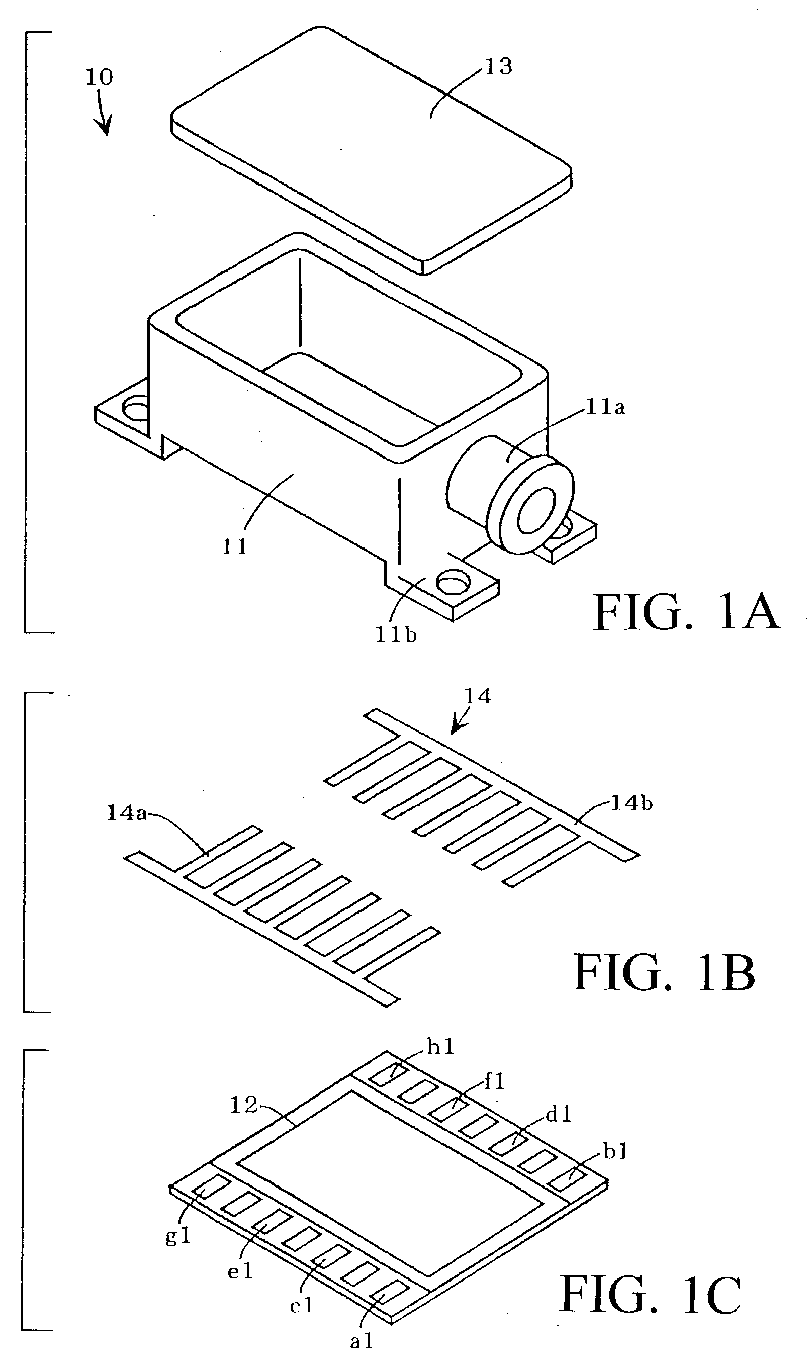
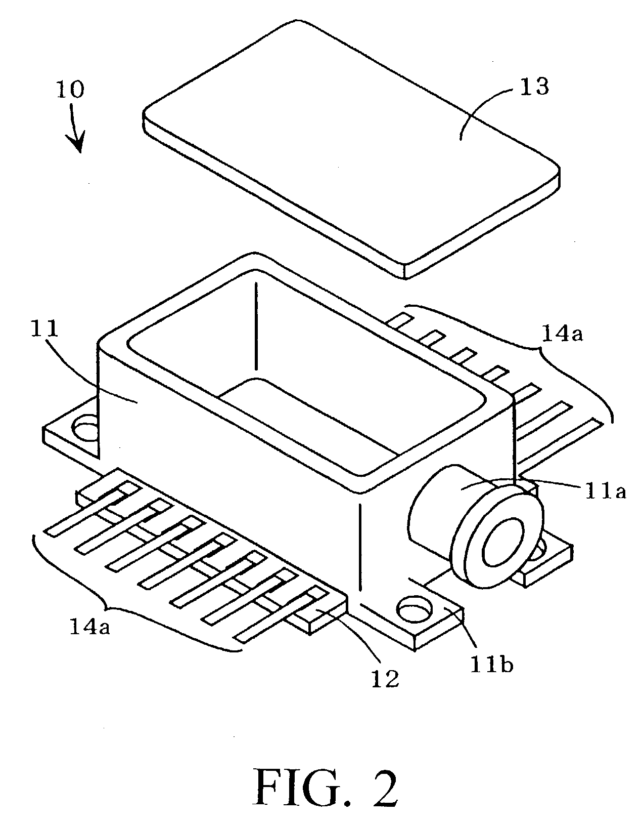
[0083] In the first embodiment described above, the external electrode patterns a1-h1 are formed on the surface of the base member 12 and are connected with the leads 14a respectively. Herein, it is possible to form external circuit electrodes on the backside or side surface of the base member 12.

[0084] In this case, internal electrode patterns a2-h2, a thermoelectric module metallizing portion i, and a frame member metallizing portion j are formed on the surface of the base member 12 as shown in FIG. 5A, while external electrode patterns a1-h1 are formed on the backside of the base member 12 as shown in FIG. 5B. Thus, it is possible to produce a modified example of the base member 12 constituted by a multilayer substrate.

[0085] The aforementioned example eliminates the necessity of arranging the external electrode patterns a1-h1 on the surface of the base member 12, which can be therefore reduced in size in a planar shape. In addition, it becomes unnecessary t...

second modification

(b) Second Modification

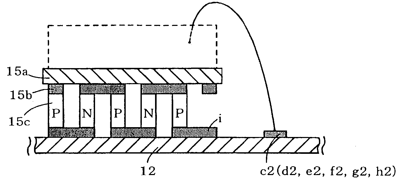
[0086] The first embodiment produces a "semi-finished" product of the thermoelectric module 15 (see FIG. 7A) in which the Peltier elements 15c join the upper substrate 15a via the electrode patterns 15b. For this reason, the thermoelectric module metallizing portion i is formed on the surface of the base member 12 in such a way that the Peltier elements 15c are arranged by alternately changing polarities thereof between p-type and n-type and are electrically connected in series.

[0087] It is possible to modify the first embodiment as shown in FIG. 7B, wherein the thermoelectric module 15 is constituted by a pair of an upper substrate 15a and a lower substrate 15e sandwiching numerous Peltier elements 15c therebetween in such a way that the Peltier elements 15c joining the upper substrate 15a via the electrode patterns 15b are arranged by alternately changing polarities thereof between p-type and n-type and are electrically connected in series while electrode pa...


PUM


Abstract

A thermoelectric module package stores a thermoelectric module for controlling temperature of a semiconductor element (e.g., a semiconductor laser) having high output power, wherein it is constituted by a frame member and a base member, on which various electrode patterns are formed. That is, the base member has internal electrodes for establishing electrical connections with the semiconductor element and thermoelectric module, and external electrodes for establishing electrical connections with external circuitry. Due to such an integrated arrangement of electrode patterns on the base member, it is possible to reduce the number of parts required for manufacturing the thermoelectric module package, which can be therefore manufactured with ease and at a relatively low cost. Incidentally, the thermoelectric module package can be produced by integrally combining a frame and a base together.

Description

[0001] 1. Field of the Invention[0002] This invention relates to semiconductor elements such as semiconductor lasers used in optical communication apparatuses, and in particular, to packages for storing thermoelectric modules performing temperature controls on semiconductor elements.[0003] 2. Description of the Related Art[0004] Recently, there are increasing needs for performing high-speed communications of large amounts of data or information as technologies regarding network systems such as the Internet have been rapidly developed and spread worldwide. Large amounts of data or information can be transmitted at a high speed by way of existing optical fiber networks, which are rapidly expanded and are frequently used in recent years. That is, so-called broadband optical networking technologies such as wavelength division multiplexing (WDM) and dense wavelength division multiplexing (DWDM) are adapted to multiplexing over channels with respect to optical signals or beams transmitted...

Claims


Application Information

Patent Timeline
Patent Type & Authority Applications(United States)
IPC IPC(8): H01L23/02H01L23/38H01L23/34H01L35/30H01L35/34H01S5/0232H01S5/024
CPCH01L23/38H01S5/02216H01S5/02415H01L2224/48091H01L2924/00014H01S5/0231H01S5/0232
Inventor ONOUE, KATSUHIKO
Owner YAMAHA CORP
Why Eureka
Try Eureka