Optical modulator, optical waveguide device and acousto-optic tunable filter apparatus

a technology of optical waveguide and optical modulator, which is applied in the direction of optical light guide, optical waveguide light guide, etc., can solve the problem that the performance improvement of the device itself may be hindered

Inactive Publication Date: 2003-11-27
FUJITSU LTD
View PDF9 Cites 31 Cited by
  • Summary
  • Abstract
  • Description
  • Claims
  • Application Information

AI Technical Summary

Problems solved by technology

However, in such a conventional optical waveguide device as described above, a great difference exists between a propagation mode in the input and output waveguides and a propagation mode in the waveguide coupling element, and therefore, there is a subject that an radiation mode appear.
Further, also where an optical w

Method used


Image

  • Optical modulator, optical waveguide device and acousto-optic tunable filter apparatus
  • Optical modulator, optical waveguide device and acousto-optic tunable filter apparatus
  • Optical modulator, optical waveguide device and acousto-optic tunable filter apparatus

Examples


first embodiment

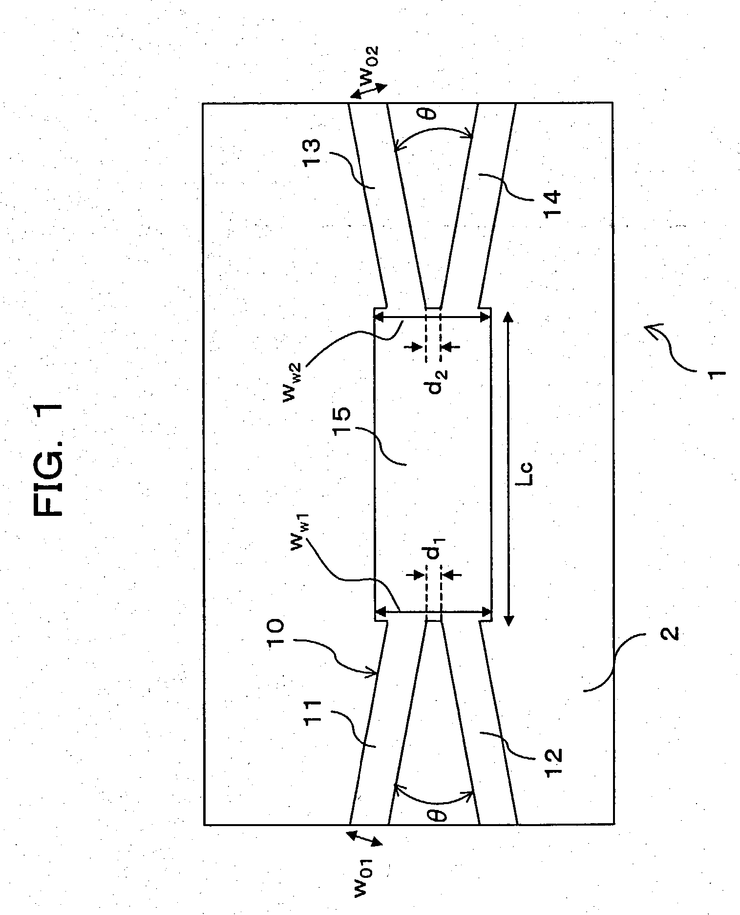
[0067] FIG. 1 is a schematic top plan view showing an optical waveguide device 1 according to the present invention. The optical waveguide device 1 shown in FIG. 1 includes a substrate 2 having an electro-optical effect and an optical waveguide 10 formed on the substrate 2. The optical waveguide 10 includes two input waveguides 11 and 12, two output waveguides 13 and 14, and a waveguide coupling element 15.

[0068] Here, the input waveguides 11 and 12 propagate lights incoming to the optical waveguide device 1, and the waveguide coupling element 15 is connected to the two input waveguides 11 and 12 with a distance d.sub.1 therebetween and causes the lights propagating in the two input waveguides 11 and 12 to interfere with each other. Further, the output waveguides 13 and 14 are branched with another distance d.sub.2 from the waveguide coupling element 15 and propagate the lights caused to interfere with each other by the waveguide coupling element 15.

[0069] Further, the waveguide cou...

second embodiment

[0114] [B] Description of the Second Embodiment

[0115] FIG. 10 is a schematic view showing an optical modulator according to a second embodiment of the present invention. In the optical modulator 100 shown in FIG. 10, reference numeral 101 denotes a substrate having an electro-optical effect and formed from lithium niobate or the like, and the substrate may have, for example, a width of 1 to 2 mm and a length of 80 to 90 mm in a longitudinal direction.

[0116] Further, reference numeral 110 denotes a Mach-Zehnder type optical waveguide mounted on the substrate 101. The Mach-Zehnder type optical waveguide 110 branches input light into two lights with a ratio of 1:1 and multiplexes the light modulated by a signal electrode section 120 and a bias electrode section 130 to output multiplexed light as modulated signal light, and includes a branching waveguide 111, linear waveguides 112 and 113 and a multiplexing waveguide 114.

[0117] Further, the branching waveguide 111 of the Mach-Zehnder ty...

third embodiment

[0177] [C] Description of the Third Embodiment

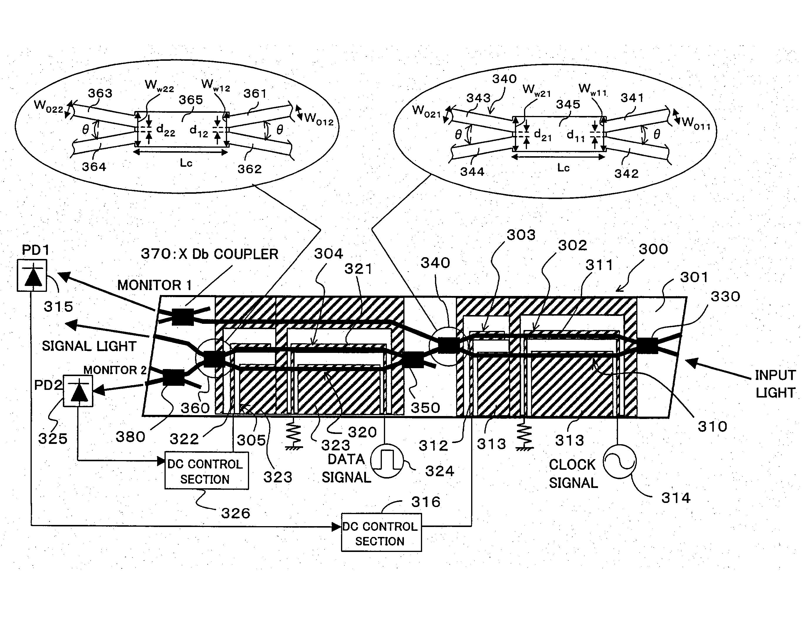
[0178] FIG. 14 is a block diagram showing an optical modulator according to a third embodiment of the present invention. In the optical modulator 300 shown in FIG. 14, when compared with the optical modulators 100 and 200 in the second embodiment described above, two Mach-Zehnder type optical waveguides 310 and 320 are formed in series on a single substrate 301 having an electro-optical effect. Further, the Mach-Zehnder type optical waveguide 310 is used for clock modulation, and the other Mach-Zehnder type optical waveguide 320 is used for data modulation.

[0179] Here, in the optical modulator 300 shown in FIG. 14, reference numeral 302 denotes a first signal electrode section. The first signal electrode section 302 is provided on the first Mach-Zehnder type optical waveguide 310 and is supplied with a clock signal, and includes a signal electrode 311 and a ground electrode 313. In particular, a clock signal source 314 is connected to th...


PUM


Abstract

The invention provides an optical modulator wherein appearance of radiation mode light can be suppressed to improve performances as a device. The optical modulator includes a multiplexing waveguide which in turn includes two input waveguides to which propagation lights from a linear waveguide are inputted, a waveguide coupling element, and two output waveguides. The width of the waveguide coupling element on the input side is greater than the total width of the two input waveguides, and the width of the waveguide coupling element on the output side is greater than the total width of the two output waveguides. The device of the present invention is applied typically to an optical communication system.

Description

[0001] 1. Field of the Invention[0002] This invention relates to an optical modulator and an optical waveguide device suitable for use with an optical communication system.[0003] 2. Description of the Related Art[0004] FIG. 16 is a schematic view showing a conventional optical multiplexer / demultiplexer having two inputs and two outputs. The optical multiplexer / demultiplexer 700 shown in FIG. 16 includes two input waveguides 702 and 703, a waveguide coupling element 706 and two output waveguides 704 and 705 formed on a substrate 701. The optical multiplexer / demultiplexer 700 can multiplex or demultiplex, when input light propagating in the input waveguides 702 and / or 703 is to be outputted to the output waveguides 704 or / and 705 through the waveguide coupling element 706, the input light.[0005] In the optical multiplexer / demultiplexer 700, for example, input light P.sub.0 inputted to the input waveguide 702 is demultiplexed into and outputted as output lights P.sub.1 and P.sub.2 from...

Claims


Application Information

Patent Timeline
IPC IPC(8): G02B6/125G02B6/28G02F1/01G02B6/12G02F1/035G02F1/11G02F1/313
CPCG02B6/2813G02B2006/12147G02F1/116G02F2201/16G02F1/3136G02F2001/217G02F1/225G02F1/217G02B6/125
Inventor DOI, MASAHARUMIYAWAKI, SHUUICHIISHIZAKA, TETSUO
Owner FUJITSU LTD
Why Eureka
Try Eureka