Optical waveguide with non-uniform sidewall gratings

a technology of optical waveguides and sidewalls, applied in the direction of optical waveguide light guides, instruments, optics, etc., can solve the problems of insufficient flexibility and performance of uniform gratings, gratings of uniform strength introduce undesirable ripples in the group delay spectrum, and difficulty in achieving and controlling varied etch depths, etc., to achieve constant grating strength

Inactive Publication Date: 2004-02-26
MASSACHUSETTS INST OF TECH
View PDF6 Cites 69 Cited by
  • Summary
  • Abstract
  • Description
  • Claims
  • Application Information

AI Technical Summary

Benefits of technology

0038] FIG. 11 illustrates contours of constant grating strength, , and effective refractive index, .eta..sub.eff, as a function of waveguide and grating width for the transverse-electric (TE) mode according to the concepts of the present invention;

Problems solved by technology

Not surprisingly, many of the conventional optical communications components require gratings or periodic physical corrugations in dielectric or semiconductor waveguides.
On the other hand, for many optical devices, the flexibility and performance of uniform gratings are insufficient.
When using chirped gratings to compensate for fiber-induced dispersion, gratings of uniform strength introduce undesirable ripples in the group-delay spectrum.
Placing the grating in the top or bottom of the waveguide presents several disadvantages, particularly if the grating is an apodized grating.
Varied etch depths are difficult to achieve and control in planar processing.
Thirdly, if the duty-cycle, the ratio of grating tooth to grating space, is varied, the finest feature that can be patterned limits the minimum obtainable grating strength.
However, as noted above, for many optical devices, the flexibility and performance of uniform gratings are insufficient.

Method used


Image

  • Optical waveguide with non-uniform sidewall gratings
  • Optical waveguide with non-uniform sidewall gratings
  • Optical waveguide with non-uniform sidewall gratings

Examples


Embodiment Construction

[0043] The present invention will be described in connection with preferred embodiments; however, it will be understood that there is no intent to limit the present invention to the embodiments described herein. On the contrary, the intent is to cover all alternatives, modifications, and equivalents as may be included within the spirit and scope of the present invention as defined by the appended claims.

[0044] For a general understanding of the present invention, reference is made to the drawings. In the drawings, like reference numbering has been used throughout to designate identical or equivalent elements. It is also noted that the various drawings illustrating the present invention are not drawn to scale and that certain regions have been purposely drawn disproportionately so that the features and concepts of the present invention could be properly illustrated.

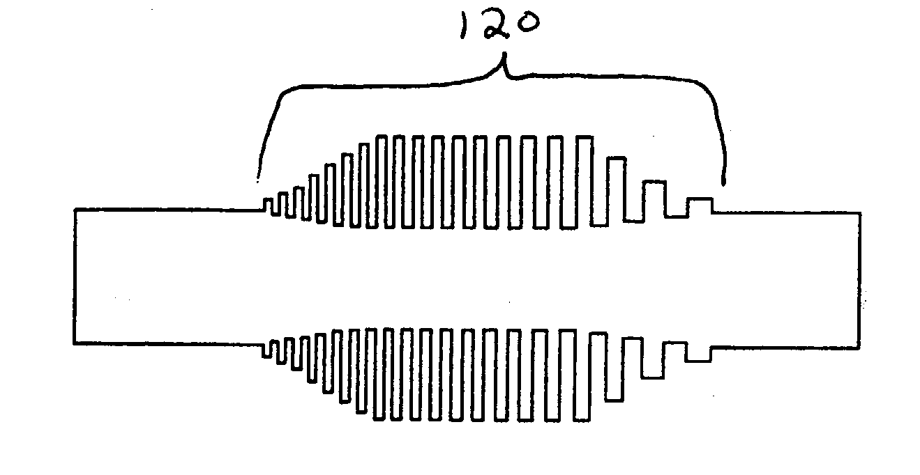
[0045] The present invention is directed to an optical device containing non-uniform gratings in an optical waveguide an...


PUM


Abstract

A diffraction grating of non-uniform strength is introduced into an optical waveguide by modulating its width. The waveguide may be fabricated using one of several planar processing techniques. Varying the size, position, and/or thickness of the grating teeth provides the desired variation of grating strength. Certain functional variations of grating strength suppress side-lobe levels in the grating reflection and transmission spectra. This process, termed apodization, is necessary for precise wavelength filtering and dispersion compensation. If desired, different periodicity gratings can be introduced in each side of the waveguide, multiple periodicities can be superimposed, the grating can be angled with respect to the waveguide, and the grating period and phase can be varied.

Description

PRIORITY INFORMATION[0001] The present patent application claims priority under 35 U.S.C. .sctn.119 from U.S. Provisional Patent Application Serial No. 60 / 384,288 filed on May 30, 2002. The entire contents of U.S. Provisional Patent Application Serial No. 60 / 384,288 filed on May 30, 2002 are hereby incorporated by reference.FIELD OF THE PRESENT INVENTION[0002] The present invention is directed to optical waveguides with non-uniform grating structures formed by varying the width of the waveguide. More particularly, the present invention is directed to a process and methodology of lithographically fabricating the waveguides and grating structures.BACKGROUND OF THE PRESENT INVENTION[0003] Conventionally, optical data transmission has been used to meet the demand of high-bandwidth, long-distance communications. As these communications networks grow in complexity, the networks will increasingly rely on compact, integrated, and manufacturable components that manipulate signals in the opti...

Claims


Application Information

Patent Timeline
Patent Type & Authority Applications(United States)
IPC IPC(8): G02B6/12G02B6/124
CPCG02B6/124G02B2006/12107G02B2006/121G02B2006/12097
Inventor HASTINGS, JEFFREY T.LIM, MICHAEL H.SMITH, HENRY I.
Owner MASSACHUSETTS INST OF TECH
Why Eureka
Try Eureka