Optical spot grid array printer

a grid array printer and optical spot technology, applied in the field of optical spot grid array printers, can solve the problems of increasing the difficulty and cost of masks used in image-projection systems, the inability to amortize the cost of masks over a large number of devices, and the time delay in making masks, so as to achieve fast mask making and wafer lithography, high data rate, and high resolution

Inactive Publication Date: 2005-05-24
APPLIED MATERIALS INC
View PDF93 Cites 58 Cited by
  • Summary
  • Abstract
  • Description
  • Claims
  • Application Information

AI Technical Summary

Benefits of technology

[0011]The present invention provides a high resolution and high data-rate direct-write spot grid array lithography system suitable for fast mask making and wafer lithography. According to the present invention, an image is exposed on a substrate by scanning a two-dimensional array of optical beams across the substrate. The image is formed by selectively modulating the optical beams the beam array is scanned across to the substrate. In alternative embodiments, Spatial Light Modulators provide for grey level modulation, in which intermediate level of signals, other than “on” and “off” are available. One such modulator is available from Franhaufer Institute, Dresden, Germany, and is referred to as a Cantilever Beam Micromirror Spatial Light Modulator. Another method for providing grey level modulation is described by Davidson, Mark, SPIE VOL. 3048, PP. 346-355, 1997 cited above. This method uses Michelson interferometer to generate gray level modulation. As described herein, “on” and “off”...

Problems solved by technology

Unfortunately, due to decreasing design rules and the wide use of RET (Resolution Enhancement Techniques) such as OPC (Optical Proximity Correction) and PSM (Phase Shift Masks), the masks used in image-projection systems have become increasingly difficult and expensive to make.
Since many masks are needed to form the multiple patterns required to manuf...

Method used


Image

  • Optical spot grid array printer
  • Optical spot grid array printer
  • Optical spot grid array printer

Examples


Embodiment Construction

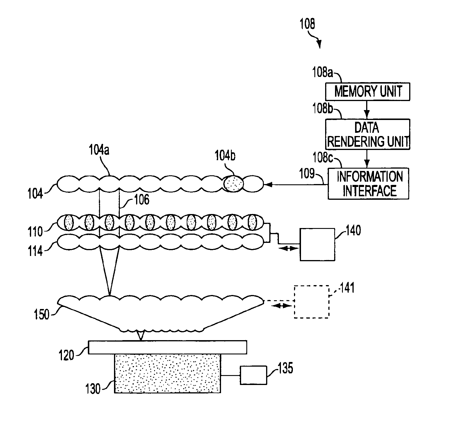
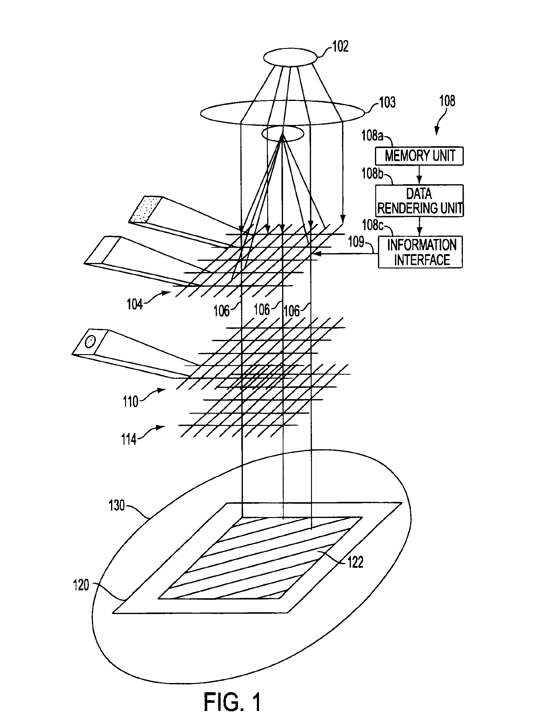
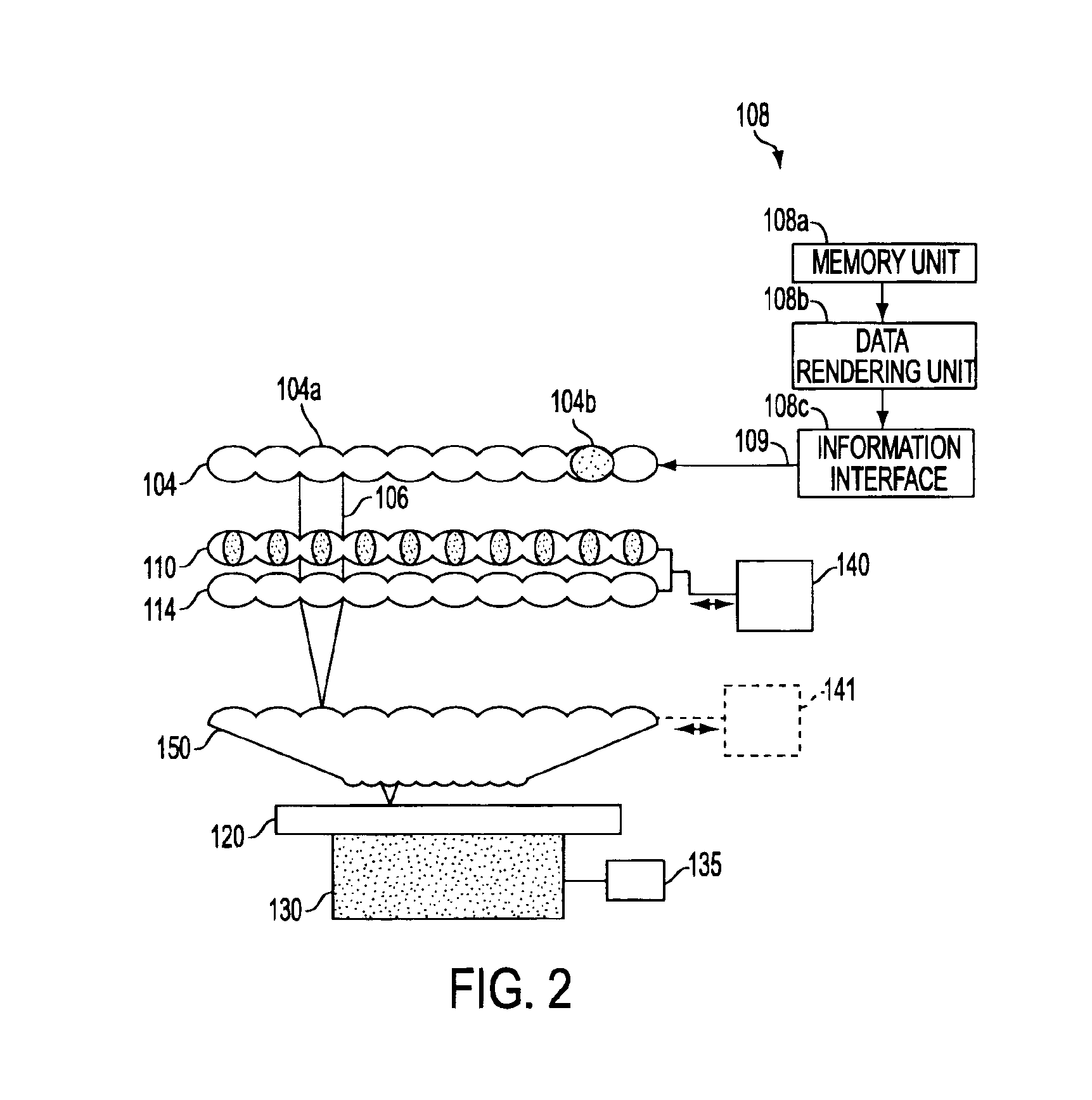
[0031]FIG. 1 illustrates a printer according to a first embodiment of the present invention. The printer includes a light source 102, which may be a continuous wave laser or a pulsed laser, collimating optics 103, and a spatial light modulator (SLM) 104, for providing and modulating a two-dimensional array of parallel optical beams 106. Spatial light modulator 104 modulates light beams in response to an input data signal 109 provided by programmable image generator 108 and controls the individual beams in synchronism with the control of stage 130 for exposure of a desired pattern onto substrate 120. The printer further includes a beam shaper array 110, interposed between spatial light modulator 104 and substrate 120, for narrowing each of the optical beams 106 for improved resolution. Focusing optics 114 provides a lens element for each beam 106 and focuses each beam onto a small spot on substrate 120 to form a grid-array of spaced-apart small spots on substrate 120. Substrate 120 i...


PUM


Abstract

A high resolution and high data rate spot grid array printer system is provided, wherein an image is formed by scanning spot-grid array of optical beams across a substrate layered with a resist. High resolution is achieved by apodizing the optical beams to provide a narrower main lobe. Unwanted recordation of side lobes upon the substrate is prevented by assuring that the side lobes do not include energy above the threshold of the resist, using a memoryless resist, and by using a slanted and interleaved scan pattern adapted for use with the spot-grid array pattern and the memoryless characteristic of the resist.

Description

CLAIM OF PRIORITY FROM PROVISIONAL APPLICATION[0001]This application claims priority from the U.S. provisional application No. 60 / 331,029 filed on Nov. 7, 2001.FIELD OF THE INVENTION[0002]The present invention refers to a maskless method and device for patterning high-resolution images directly on photolithographic layers with a massively-parallel beam array. This device is intended for use in the fabrication of semiconductor devices, microelectronics, Microsystems, thin-film devices, flat screens, and the structuring of masks and substrates for microlithographic applications.BACKGROUND ART[0003]Photolithography is a technique for transferring images onto semiconductor or other substrates. There are two fundamental types of photolithography systems. A first type, referred to as image-projection lithography, uses master patterns, referred to as masks or reticles, and a projection system for projecting the image on the mask on a substrate. A second type of system, referred to as a mas...

Claims


Application Information

Patent Timeline
IPC IPC(8): G03F7/20
CPCG03F7/2057G03F7/70391G03F7/70291G03F7/70275G03F7/7005
Inventor ALMOGY, GILAD
Owner APPLIED MATERIALS INC
Why Eureka
Try Eureka