Process for the transfer of a thin film comprising an inclusion creation step

a transfer process and a technology for inclusions, applied in the direction of solid-state device manufacturing, electric devices, semiconductor/solid-state device manufacturing, etc., can solve the problems of unsatisfactory film surface planeness after separation and inability to maintain a uniform thickness of thin film

Inactive Publication Date: 2004-03-25
COMMISSARIAT A LENERGIE ATOMIQUE ET AUX ENERGIES ALTERNATIVES
View PDF50 Cites 20 Cited by
  • Summary
  • Abstract
  • Description
  • Claims
  • Application Information

AI Technical Summary

Problems solved by technology

The planeness of the film surface obtained after separation is unsatisfactory, an...

Method used


Image

  • Process for the transfer of a thin film comprising an inclusion creation step
  • Process for the transfer of a thin film comprising an inclusion creation step
  • Process for the transfer of a thin film comprising an inclusion creation step

Examples


Embodiment Construction

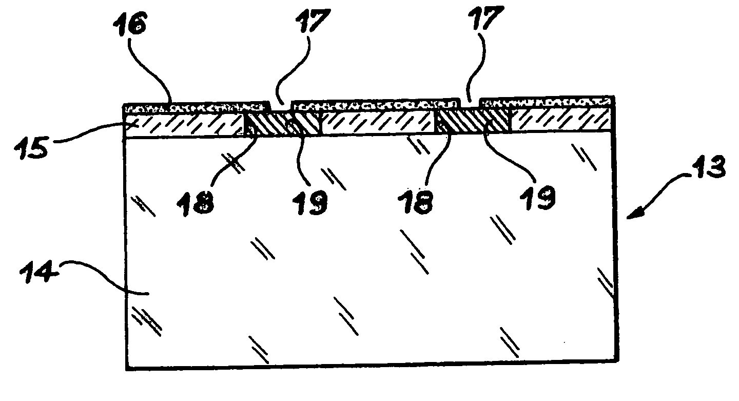
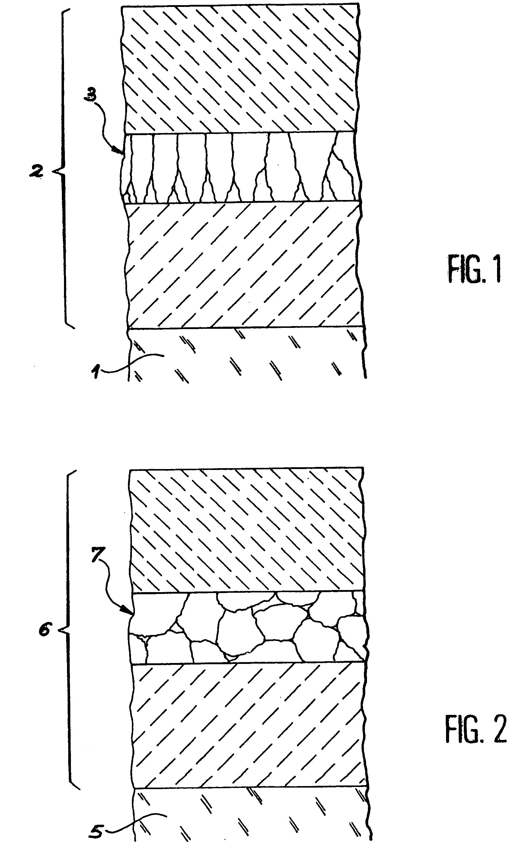
[0009] The improvement proposed by this invention is made possible due to creation of an inclusion or a set of inclusions in the initial substrate material, in order to confine gaseous compounds introduced during the ion implantation step. An inclusion is a volume of material for which the properties are not the same as the properties of the substrate material from which one or more thin films are to be transferred. Inclusions may be in the form of a layer that extends approximately parallel to the surface through which the implantation is done. These volumes may have a variety of shapes and their dimensions may vary from a few tens of nanometers to several hundreds of micrometers.

[0010] The role of these inclusions is to act as traps for implanted gaseous compounds. The radius of action of these traps depends on the nature of the inclusions made. In this case, there is no removed material, as is the case for the process divulged by document EP-A-0 767 486.

[0011] The process accordi...


PUM


Abstract

This invention relates to a process for transfer of at least one thin film of solid material delimited in an initial substrate (20). It comprises the following steps: a step in which a layer of inclusions (21) is formed in the initial substrate (20) at a depth corresponding to the required thickness of the thin film, these inclusions being designed to form traps for gaseous compounds which will subsequently be implanted; a subsequent step for implantation of the said gaseous compounds, in a manner to convey the gaseous species into the layer of inclusions, the dose of implanted gaseous compounds being sufficient to cause the formation of micro-cavities likely to form a fracture plane along which the thin film can be separated from the remainder of the substrate.

Description

TECHNICAL DOMAIN[0001] This invention relates to a process for transferring a thin film of solid material. In particular, this process can be used to transfer a thin film of solid material onto a support composed of a solid material of the same nature or a different nature.[0002] STATE OF PRIOR ART[0003] Document FR-A-2 681 472 (corresponding to patent U.S. Pat. No. 5,374,564) describes a process for making thin films of semiconducting material. This document divulges that the implantation of a rare gas or hydrogen into a substrate made of a semiconducting material can cause the formation of a layer of micro-cavities or micro-bubbles (also denoted "platelets") at a depth close to the average projected range (Rp) of the implanted ions. The concept of micro-cavities obviously includes micro-cracks. The thickness of the layer of micro-cavities is determined by the implantation conditions. If this substrate is put into intimate contact with a stiffener through its implanted face and a h...

Claims


Application Information

Patent Timeline
IPC IPC(8): H01L21/02H01L21/265H01L21/762H01L27/12
CPCH01L21/26506Y10S438/977H01L21/76254H01L21/265
Inventor MORICEAU, HUBERTBRUEL, MICHELASPAR, BERNARDMALEVILLE, CHRISTOPHE
Owner COMMISSARIAT A LENERGIE ATOMIQUE ET AUX ENERGIES ALTERNATIVES
Why Eureka
Try Eureka