

System-in-a-package device
- Summary
- Abstract
- Description
- Claims
- Application Information
AI Technical Summary
Benefits of technology
Problems solved by technology
Method used
Image

Examples
Embodiment Construction
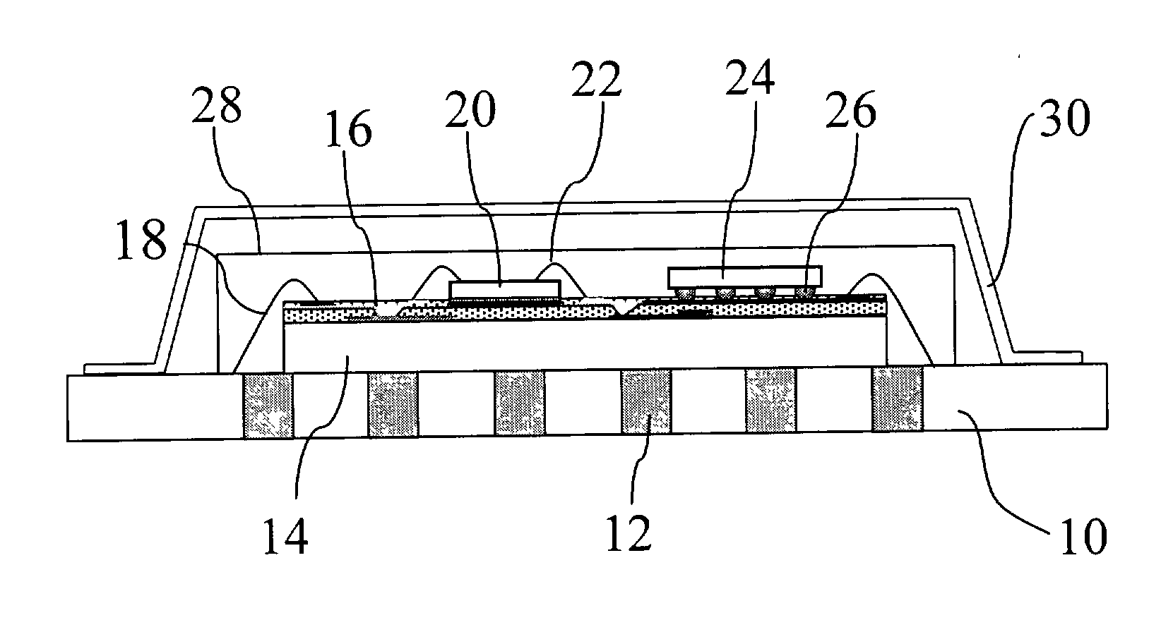
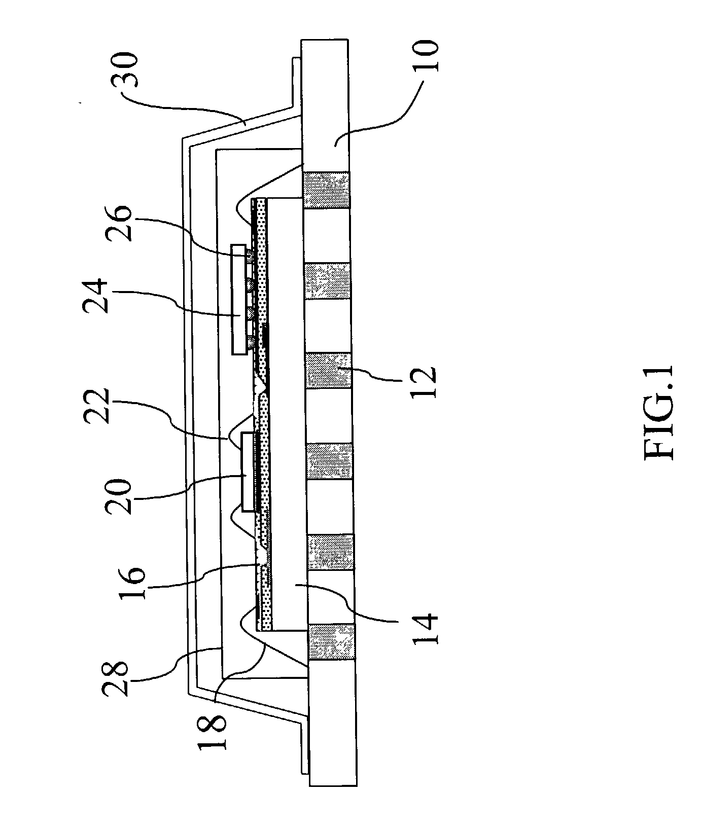
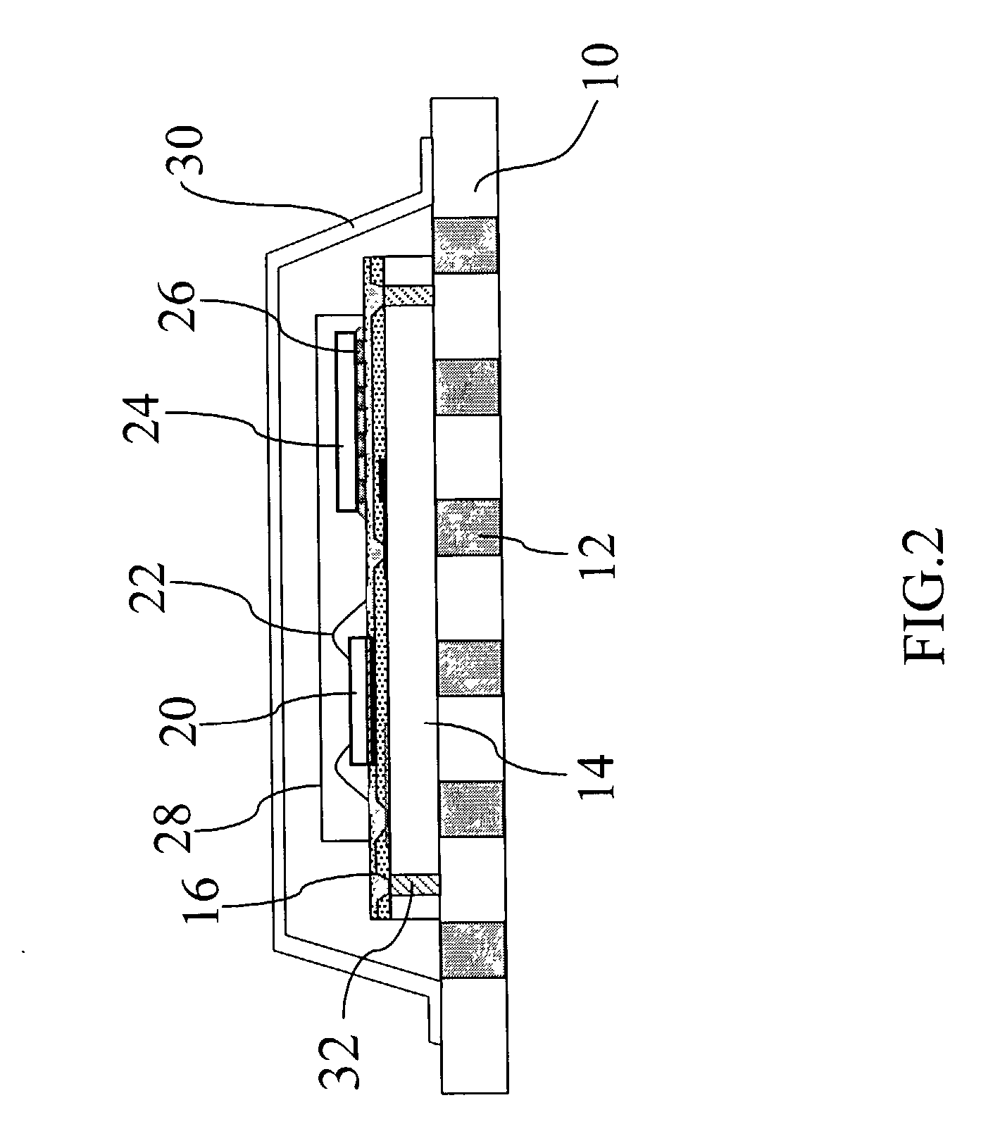
[0017] The present invention directly integrates integrated passive devices (IPD) like resistors, capacitors, or inductors into a substrate, and then installs at least an active device on the surface of the IPD substrate, thereby accomplishing a system package integrating all circuits on ICs and thus effectively resolving the drawbacks in the prior art.
[0018] As shown in FIG. 1, a system-in-package device comprises a bearing substrate 10, which has several through conducting holes 12 thereon. An IPD substrate 14 with a plurality of passive devices 16 formed thereon is also provided. The IPD substrate 14 has a first surface and a second surface. The second surface of the IPD substrate 14 is installed on the surface of the bearing substrate 10. A plurality of wires 18 are used to achieve electric connection between the IPD substrate 14 and the bearing substrate 10 by means of wire bonding. Two active devices (a first active device 20 and a second active device 24) like semiconductor c...
PUM
 Abstract
Description
Claims
Application Information