Manufacturing method for electronic component module and electromagnetically readable data carrier

a manufacturing method and data carrier technology, applied in resist details, instruments, printed circuit aspects, etc., can solve the problems of increasing manufacturing costs, requiring 10 to 20 seconds to cure resin materials, and increasing the cost of anisotropic conductive sheets g, etc., to achieve low cost and low cost

Inactive Publication Date: 2004-06-17
ORMON CORP
View PDF8 Cites 14 Cited by
  • Summary
  • Abstract
  • Description
  • Claims
  • Application Information

AI Technical Summary

Benefits of technology

][0185] As will be apparent from the above description, with this invention, it is possible to provide the method for manufacturing the electronic component module in which the semiconductor bear chip is packaged on the wiring board rapidly in electrically and mechanically reliable way and at low cost, in which it is possible to prevent a short-circuit from occurring due to a contact between the semiconductor bear chip and the electrode area on the wiring board even in a situation where a high temperature and high pressure load is applied on the packaged portion of the semiconductor bear chip.[0186] With the invention, it is possible to provide the method for manufacturing the electromagnetically readable data carrier at low cost and in mass production, in which the electromagnetically readable data carrier serves as an aircraft tag, a physical distribution management label, or an unmanned wicket pass.

Problems solved by technology

The first method has several problems that (1) a process for supplying and curing the bonding material e for connecting the bump b and the electrode area d on the wiring pattern is complex, (2) a process for filling an insulating resin f called an under-fill between the chip a and the wiring board c and sealing a bump connecting portion is required to obtain a reliable moisture resistance of the bump connecting portion and a mounting strength of semiconductor, and (3) a process for filling and curing the insulating resin f as the under-fill is needed, thereby increasing the manufacturing cost.
On the contrary, there are still several problems that (1) the anisotropic conductive sheet g is relatively expensive, (2) the temperature higher than 200.degree. C. is required for curing to disable the less heat-resistant board, (3) it takes 10 to 20 seconds to cure the resin material, though it is a relatively short time.
It is difficult to simplify and make faster the process, and (4) the electrical connection between the bump and the wiring pattern is made by the contact of conductive particles dispersed in the resin material, with poor reliability of connection.
However, this third conventional method has the following problems.
That is, since the holes are produced within the thermosetting resin film, the thermosetting resin film is fragile in durability, whereby the bump is easily inserted through the thermosetting resin film.
When it is required to cut the wiring board depending on the uses, there is a risk of shorting the life of a cutter knife, if hard particles of oxides such as silicone oxide or aluminum oxide are included in the thermosetting resin film.
It has been found that the bump is difficult to insert through the thermosetting resin film (i.e., electrical connection between the semiconductor bear chip and the electrode area) below 10 wt %, while the work ability of the resin is degraded beyond 30%.

Method used


Image

  • Manufacturing method for electronic component module and electromagnetically readable data carrier
  • Manufacturing method for electronic component module and electromagnetically readable data carrier
  • Manufacturing method for electronic component module and electromagnetically readable data carrier

Examples


Embodiment Construction

[0083] [Embodiments]

[0084] A method for manufacturing an electronic component module according to a preferred embodiment of the present invention will be described below with reference to the accompanying drawings. The following embodiment constitutes only a part of the invention, but the scope of the invention may be defined only by the claims in the specification.

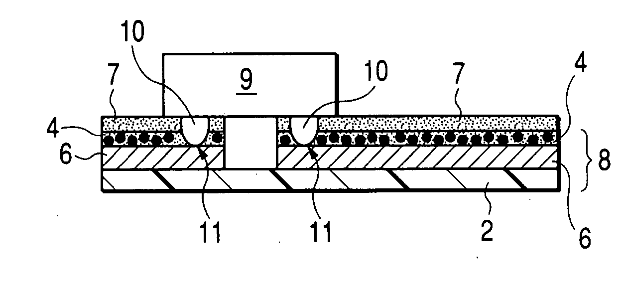
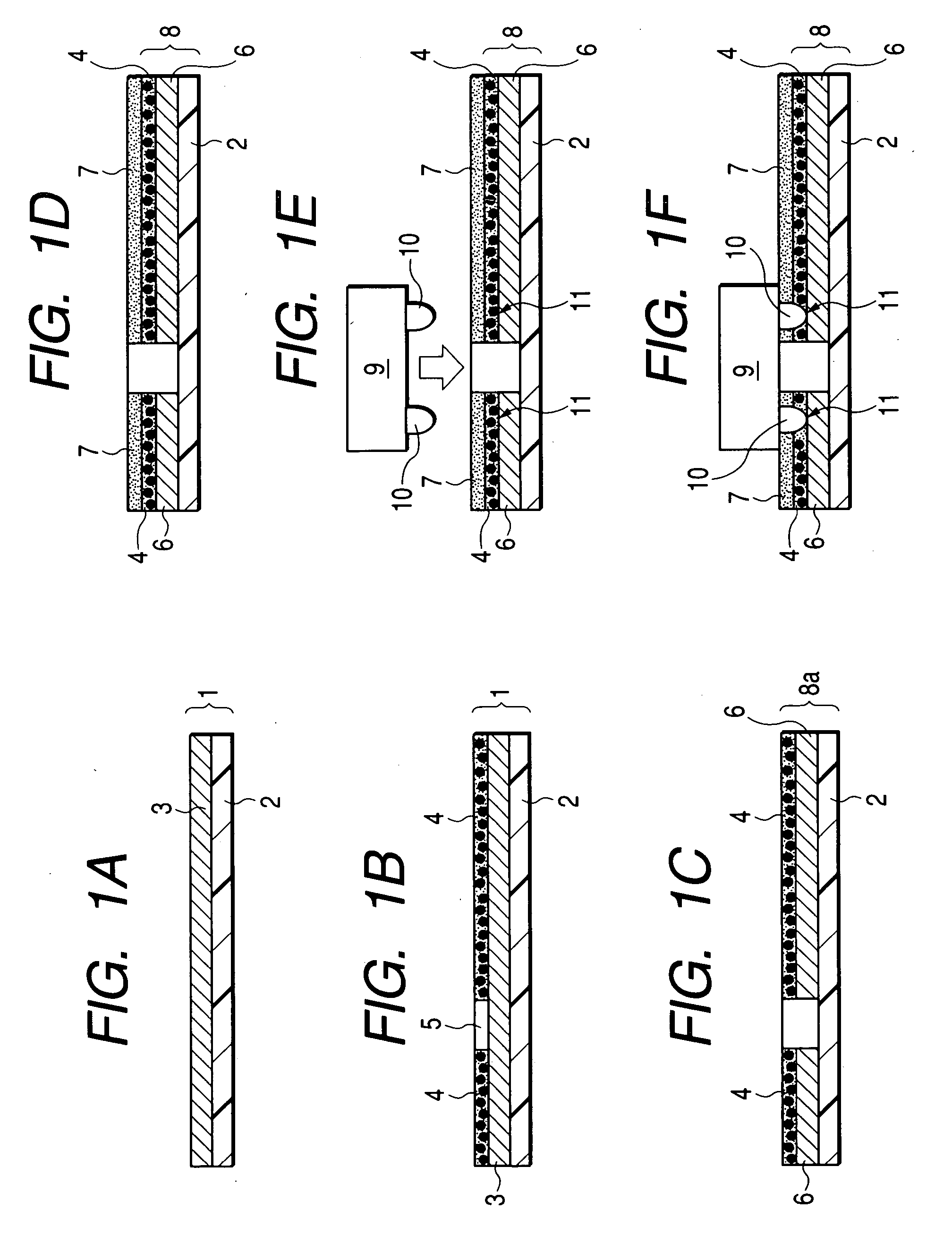
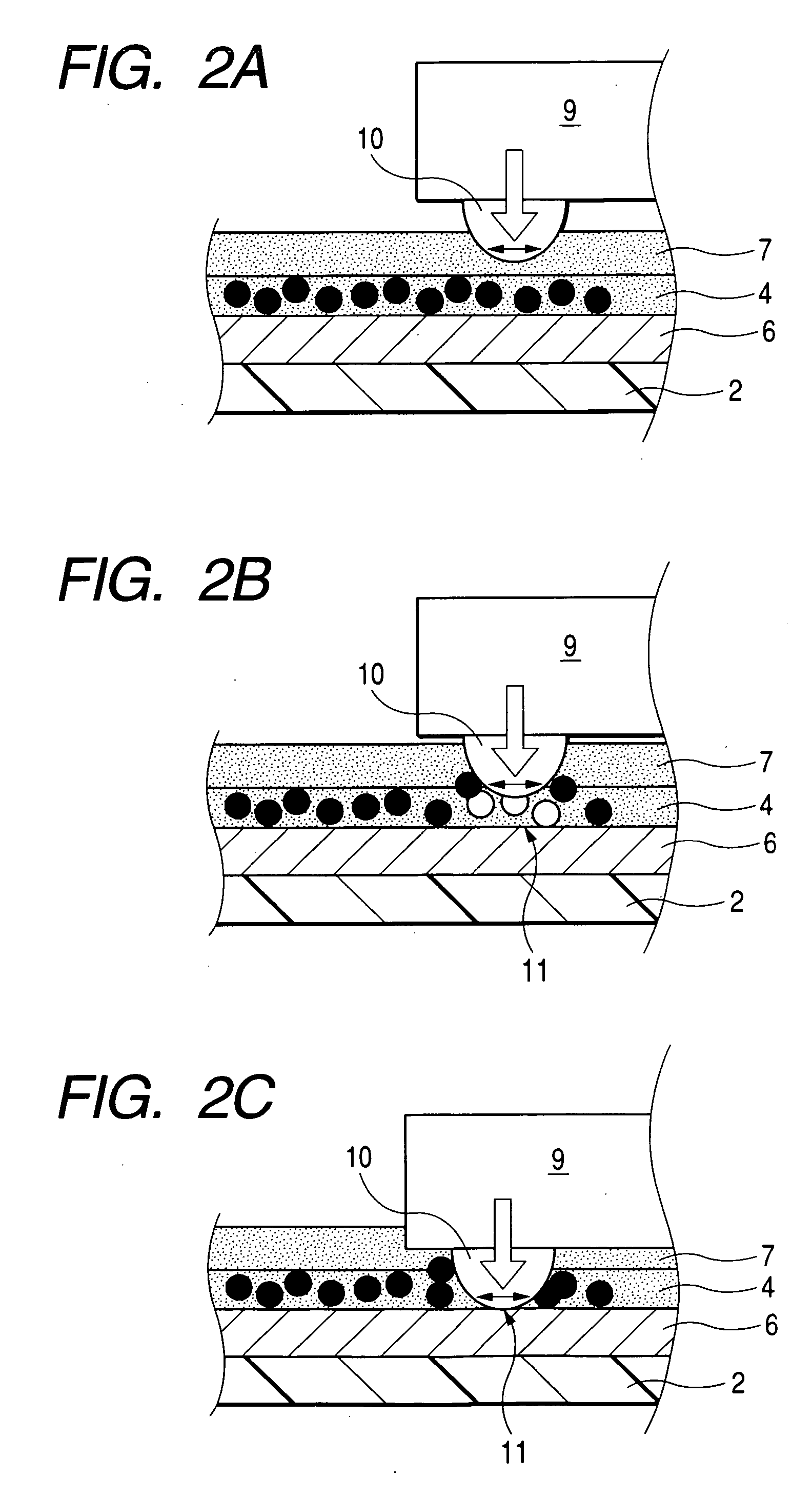
[0085] This embodiment involves a method for manufacturing an electronic component module in which a method for manufacturing an electronic component module having a semiconductor bear chip packaged on a wiring board, said method including:

[0086] preparing said wiring board including a wiring pattern, a thermosetting resin film covering an electrode area on said wiring pattern and having insulating particles dispersed and included, and a thermoplastic resin film covering said thermosetting resin film;

[0087] pressing a bump of the semiconductor bear chip onto the thermoplastic resin film in a melted state where said thermo...


PUM


Abstract

A semiconductor bear chip having a bump subjected to high temperatures is pressed, from the upper side, onto a wiring board including a wiring pattern, a thermosetting resin film covering an electrode area on the wiring pattern and having insulating particles dispersed and included and a thermoplastic resin film covering the thermosetting resin film, while applying a ultrasonic wave, thereby inserting the bumps of the semiconductor bear chip through the thermoplastic resin film and the thermosetting resin film to bond the top end portion of the bump with the electrode area.

Description

[0001] 1. Field of the Invention[0002] The present invention relates to a method for manufacturing an electronic component module that is suitable for manufacturing an electromagnetically readable data carrier operating as an aircraft tag, a physical distribution management label or an unmanned wicket pass, and more particularly to a method for manufacturing an electronic component module in which a semiconductor bear chip is packaged on a wiring board by a flip chip connecting method at low cost, in which it is possible to prevent a short circuit from occurring due to a contact of the semiconductor bear chip with an electrode area on the wiring board even under a situation where a high temperature and high pressure load is applied on a packaged portion of the semiconductor bear chip.[0003] 2. Description of the Related Art[0004] A so-called "aircraft tag" is well known as the electromagnetically readable data carrier of this type. It is expected that this aircraft tag is used in di...

Claims


Application Information

Patent Timeline
Patent Type & Authority Applications(United States)
IPC IPC(8): H05K3/32G06K19/07G06K19/077H01L21/56H01L21/60H01L21/607H01L23/498H05K3/06H05K3/30
CPCG06K19/07745G06K19/0775H01L21/563H01L23/49855H01L24/81H01L24/83H01L2224/29082H01L2224/2919H01L2224/2929H01L2224/29388H01L2224/81191H01L2224/81205H01L2224/8183H01L2224/83102H01L2224/83192H01L2224/83194H01L2224/83851H01L2224/83862H01L2224/8388H01L2224/83885H01L2224/9211H01L2224/92125H01L2924/01004H01L2924/01013H01L2924/01029H01L2924/01033H01L2924/01078H01L2924/01079H01L2924/01082H01L2924/15311H01L2924/1532H01L2924/19041H05K3/061H05K3/305H05K3/328H05K2201/0209H05K2201/0212H05K2201/10674H05K2201/10977H05K2203/0571H05K2203/1189H01L2924/01005H01L2924/01006H01L2924/01019H01L2924/01023H01L2924/01047H01L2924/01074H01L2924/01075H01L2924/014H01L2224/136H01L2224/16238H01L2924/01327H01L2223/6677H01L2224/73204H01L2224/29386H01L2224/16227H01L2224/81395H01L2224/16225H01L2924/15151H01L2224/81H01L2224/83H01L2924/05442H01L2924/00014H01L2924/0665H01L2224/0401H05K3/32
Inventor KAWAI, WAKAHIROSATO, NORIAKI
Owner ORMON CORP
Why Eureka
Try Eureka