Thermal infrared detector and infrared image sensor using the same
- Summary
- Abstract
- Description
- Claims
- Application Information
AI Technical Summary
Problems solved by technology
Method used
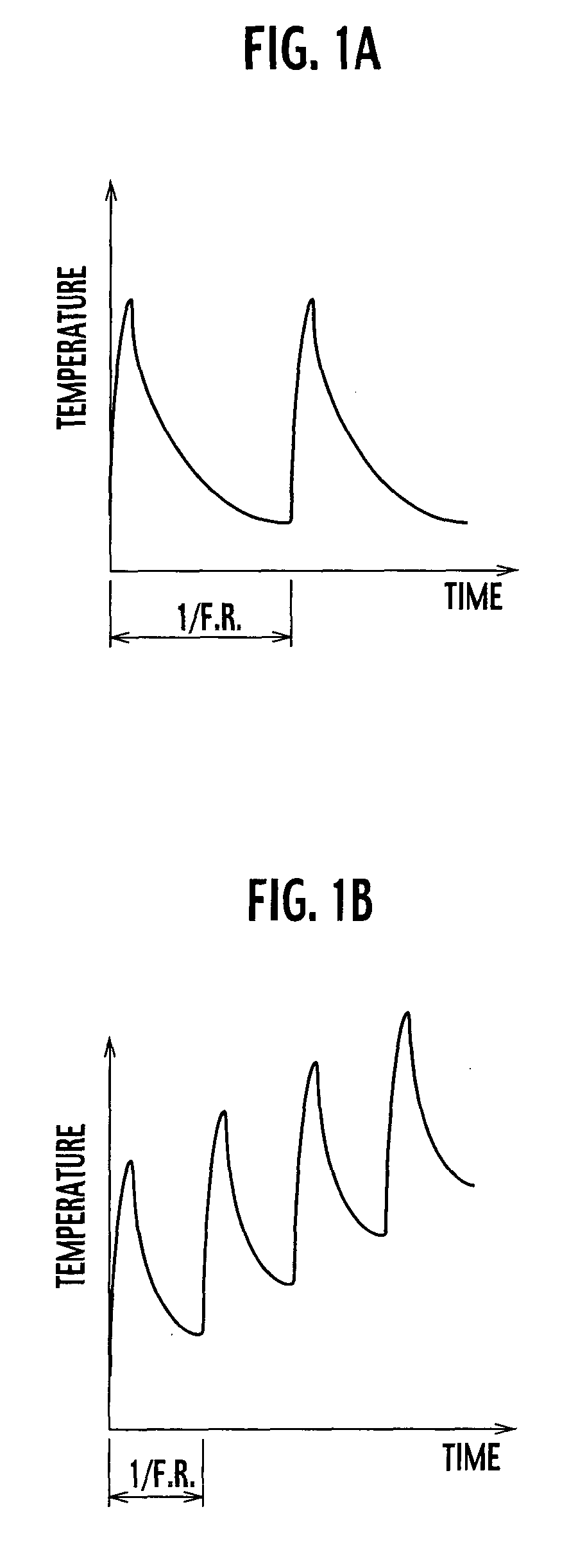
Image

Examples
first embodiment
1. First Embodiment
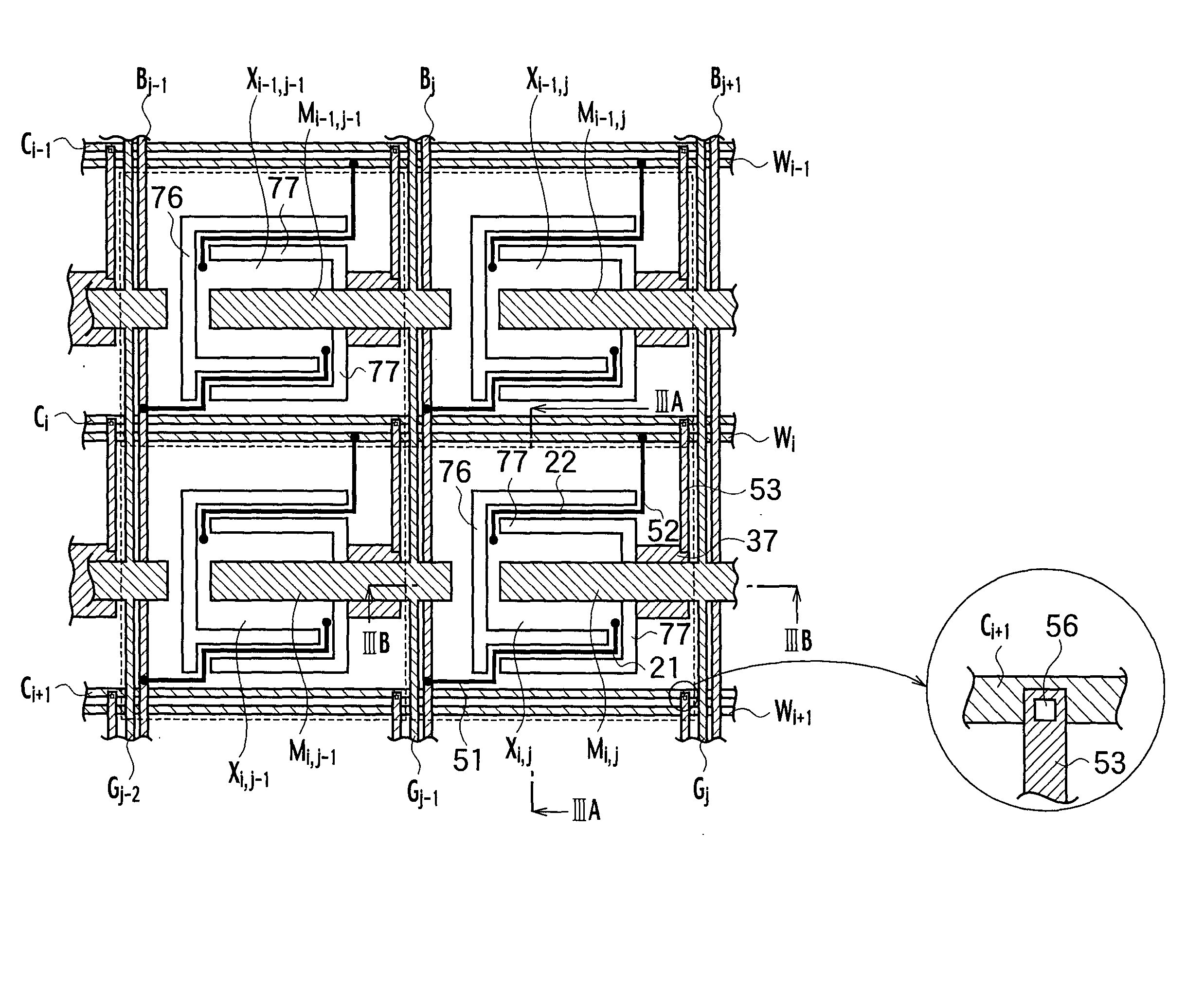
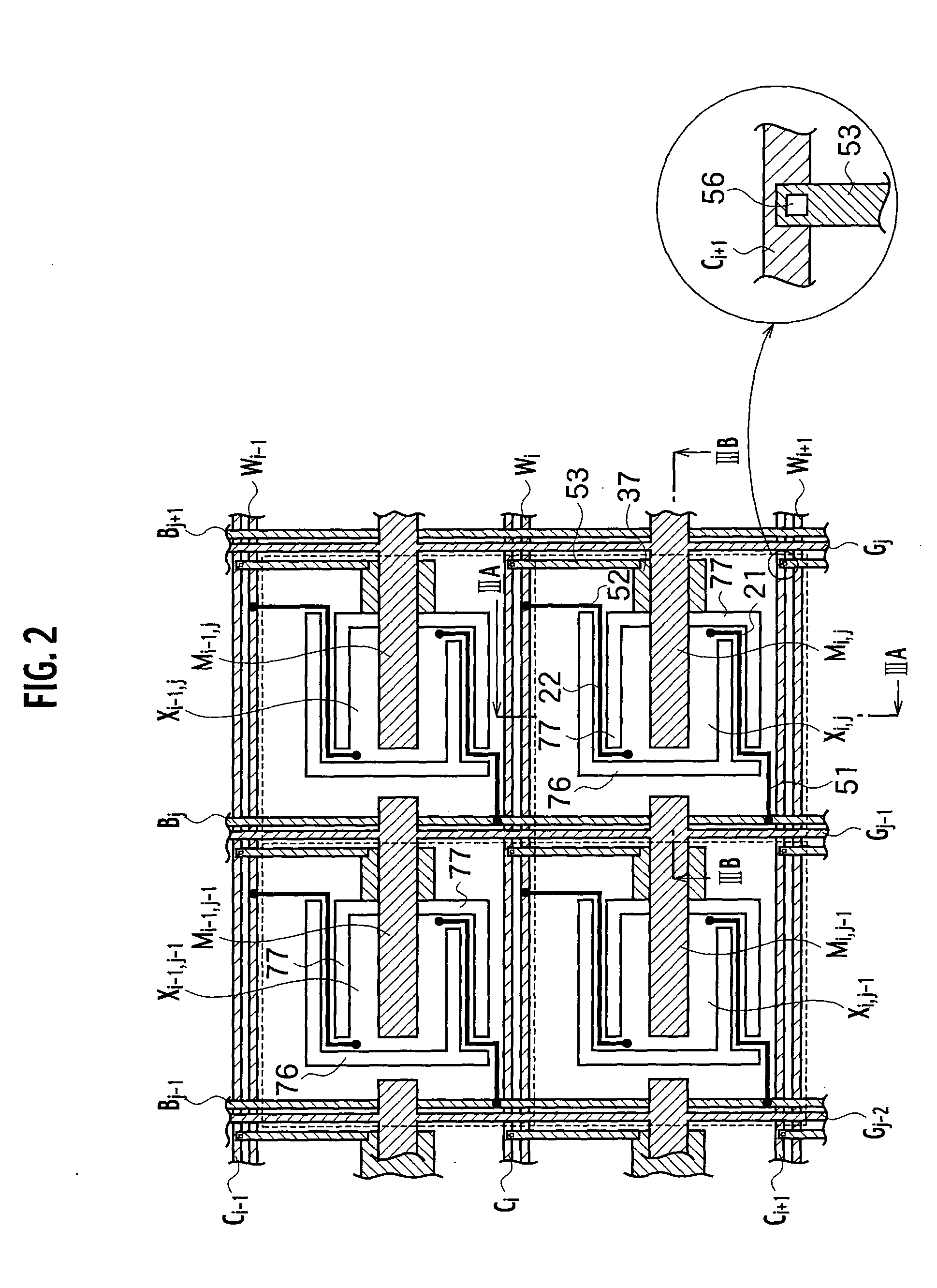
[0057] 1.1 Configuration of Infrared Image Sensor
[0058] An infrared image sensor according to the first embodiment of the present invention embraces a matrix composed by a plurality of vertical signal lines B.sub.j-1, B.sub.j, B.sub.j+1, . . . and a plurality of horizontal address lines W.sub.i-1, Wi, W.sub.j+1, . . . intersecting perpendicularly to the vertical signal lines B.sub.j-1, B.sub.j, B.sub.j+1, . . . and a plurality of detector portions X.sub.i-1,j-1, X.sub.i-1,j . . . , X.sub.i,j-1, X.sub.i,j, . . . each implementing a pixel, such that the detector portions X.sub.i-1,j-1, X.sub.i-1,j . . . X.sub.i,j-1, X.sub.i,j, . . . are arranged in a two-dimensional configuration, as shown in FIG. 2. Furthermore, in parallel with the vertical signal lines B.sub.j-1, B.sub.j, B.sub.j+1, . . . a plurality of contactor wirings G.sub.j-2, G.sub.j-1, G.sub.j, . . . extend straightforwardly. In addition, in parallel with the horizontal address lines W.sub.i-1, W.sub.i, W....
second embodiment
2. Second Embodiment
[0116] In the infrared image sensor according to the first embodiment, the control electrode 37 was disposed on the surface of the supporting substrate (the single crystalline silicon) 1, which surrounds the detector portions X.sub.i-1,j-1, X.sub.i-1,j, . . . , X.sub.i,j-1, X.sub.i,j, . . . . However, in an infrared image sensor according to the second embodiment of the present invention, the configuration of the control electrode 38 is different from the infrared image sensor according to the first embodiment, because the control electrode 38 is disposed in the inside of the detector portions X.sub.i-1,j-1, X.sub.i-1,j, . . . , X.sub.i,j-1, X.sub.i,j, . . . as shown in FIGS. 23 and 24. Although, in the second embodiment, the case in which a base body (31, 32) is implemented by a silicon substrate 31 and a pad oxide film 32 disposed on the silicon substrate 31 is described, but the base body (31, 32) can be implemented by SOI architecture, of course.
[0117] That i...
third embodiment
3. Third Embodiment
[0122] As shown in FIG. 25, a planar configuration of an infrared image sensor according to the third embodiment of the present invention, similar to the infrared image sensor according to the first embodiment, represents a plurality of control electrodes 37 being disposed on the top surface of the silicon substrate 31 surrounding a plurality of detector portions X.sub.i-1,j-1, X.sub.i-1,j, . . . , X.sub.i,j-1, X.sub.i,j, . . . That is to say, a plurality of mechanical switches of the infrared image sensor according to the third embodiment embrace respectively contactors M.sub.i-1,j-1, M.sub.i-1,j . . . , M.sub.i,j-1, M.sub.i,j, . . . , delineated in the cantilever configuration being connected electrically to corresponding contactor wirings GJ21 G.sub.j-1, G.sub.j, . . . disposed on the top surface of the base body (31, 32), each of the contactors M.sub.i-1,j-1, M.sub.i-1,j . . . , M.sub.i,j-1, M.sub.i,j, . . . has a pillar fixed to the base body (31, 32) and a f...
PUM
 Abstract
Description
Claims
Application Information