Semiconductor device and manufacturing method thereof, delamination method, and transferring method

a technology of semiconductor devices and manufacturing methods, applied in semiconductor devices, identification means, instruments, etc., can solve the problems of fragility and heaviness to be enlarged, damage to a delamination layer, and polysilicon film cannot be formed directly

Active Publication Date: 2004-07-08
SEMICON ENERGY LAB CO LTD
View PDF58 Cites 132 Cited by
  • Summary
  • Abstract
  • Description
  • Claims
  • Application Information

AI Technical Summary

Benefits of technology

[0010] A TFT formed according to the present invention can be applied to any light emitting device of top emission type or bottom emission type; or to any liquid crystal display device of transmissive type, reflective type, or semi-transmissive type; or the like.

Problems solved by technology

Glass substrates and quartz substrates are mostly used; however, they have disadvantages of fragility and heaviness to be enlarged.
However, when a sophisticated polysilicon film is used for an active layer of a TFT; a process at a high temperature at several hundred degrees centigrade is necessary in a manufacturing process, so that the polysilicon film can not be formed directly on a plastic film.
That causes a problem of damage to a delamination layer.
Further, the above publication describes a structure in which a light-resistant layer or a reflective layer is provided to prevent the damage to the delamination layer; however, in that case, it is difficult to fabricate a transmissive liquid crystal display device or a light emitting device which emits light downward.
Still further, with the above method, it is difficult to separate a delamination layer having a large area.

Method used


Image

  • Semiconductor device and manufacturing method thereof, delamination method, and transferring method
  • Semiconductor device and manufacturing method thereof, delamination method, and transferring method
  • Semiconductor device and manufacturing method thereof, delamination method, and transferring method

Examples


embodiment 1

[0067] [Embodiment 1]

[0068] In this embodiment, a result of a delamination experiment and an audit observation of a transmission electron microscope (TEM) will be described.

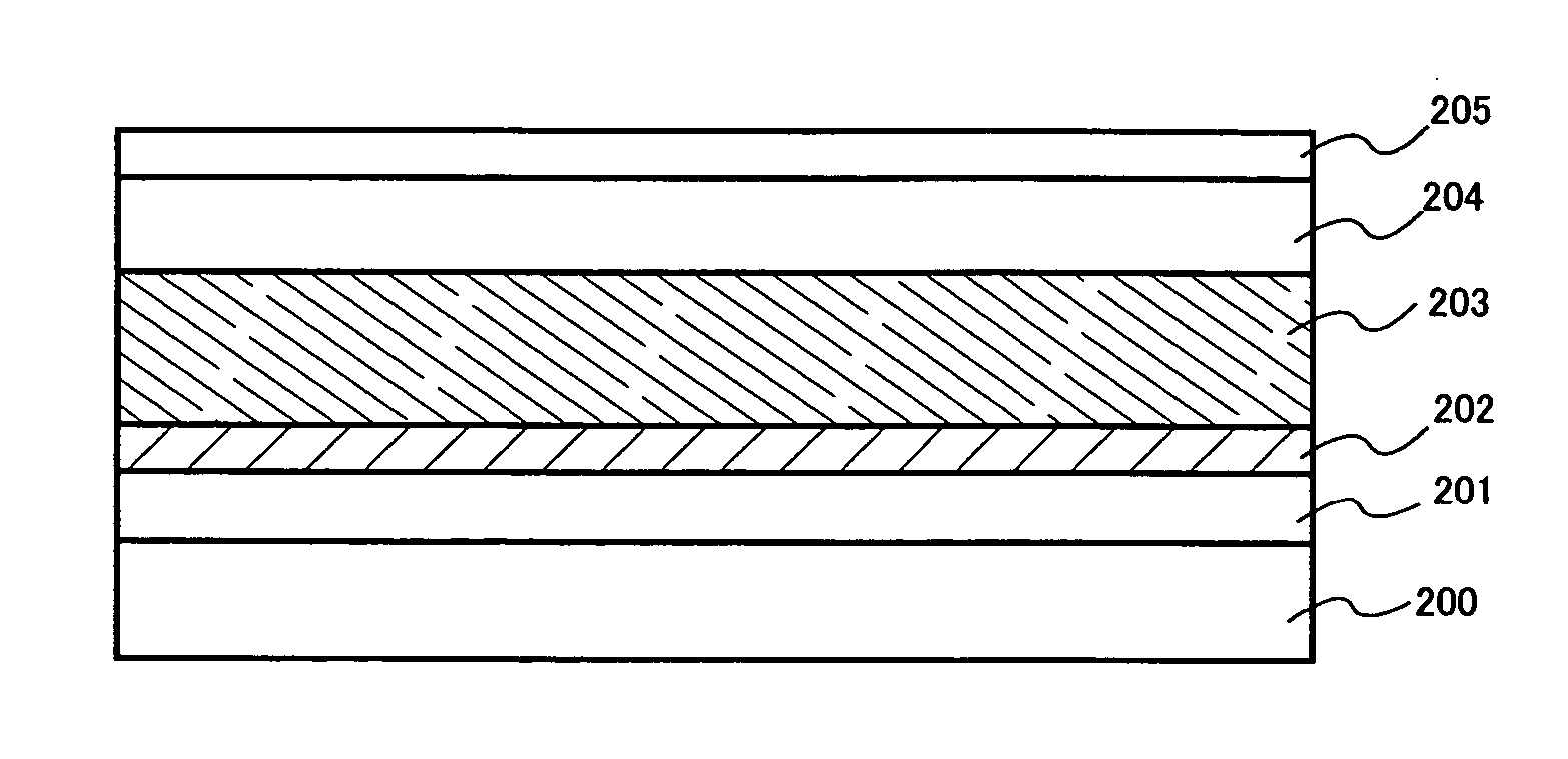
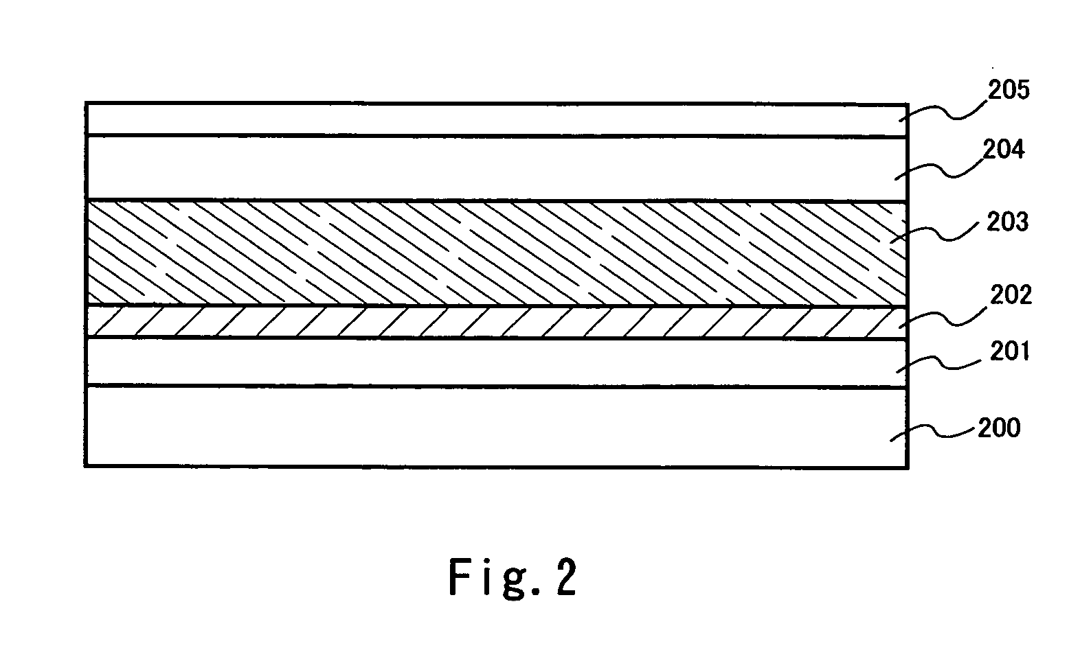
[0069] First, as to a sample shown in FIG. 2, an AN 100 glass substrate (126.times.126 mm.sup.2) as a substrate and a film mainly consisting of tungsten (hereinafter referred to as a W film) deposited by sputtering as a metal film are laminated. Thereafter, a SiO.sub.2 film deposited by sputtering as a protective film forming a delamination layer, a SiON film deposited by CVD as a base film, and an amorphous silicon film deposited by CVD as a semiconductor film are laminated thereover.

[0070] Among the above samples, one to which heat treatment is not performed shall be A, another to which heat treatment at 220.degree. C. for one hour is performed shall be B, and the other to which heat treatment at 500.degree. C. for one hour and heat treatment at 550.degree. C. for four hours thereafter are performed shall be C....

embodiment 2

[0080] [Embodiment 2]

[0081] Next, a delamination experiment is carried out under a different condition for manufacturing the protective film, or as the absence or presence of the protective film on a W film is varied.

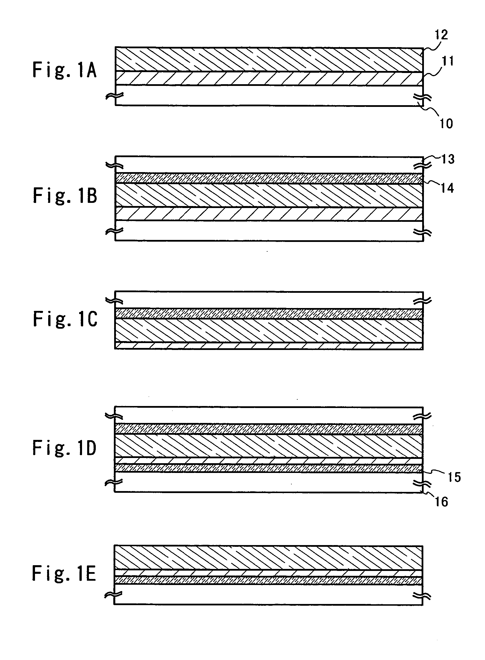
[0082] As shown in FIGS. 11A to 11D, the followings are prepared: sample 1 formed by sequentially laminating a SiON film 301 formed on a substrate 300 by CVD and a W film 302 formed by sputtering (FIG. 11A); sample 2 comprising a Si film 303 over a W film, formed by sputtering using argon gas, as a protective film (FIG. 11B); sample 3 comprising a SiO.sub.2 film 304 formed by sputtering using argon gas and oxygen gas instead of Si film (FIG. 11C); and sample 4 comprising a SiO.sub.2 film 305 formed by CVD using silane gas and nitrogen gas (FIG. 11D).

[0083] FIGS. 12A to 15A show TEM pictures of cross sections of respective samples 1 to 4. The frame formats corresponding to the respective TEM pictures are shown in FIGS. 12B to 15B.

[0084] As illustrated in FIGS. 12A to 15A...

embodiment 3

[0091] [Embodiment 3]

[0092] In this embodiment, a result of the observation of an oxide layer on the side of a substrate and the side of an amorphous semiconductor film after the separation using TEM will be shown.

[0093] A W film with a thickness of 50 nm is formed over a glass substrate by sputtering; a silicon oxide film with a thickness of 200 nm is formed thereafter by sputtering; subsequently, an silicon oxynitride film with a thickness of 100 nm is formed as a base film by plasma CVD; and an amorphous film with a thickness of 50 nm is formed as a semiconductor film likewise by plasma CVD. Then, heat treatment is performed at 500.degree. C. for 1 hour and at 550.degree. C. for 4 hours; a quartz substrate is adhered by using epoxy resin as a bond; and separation is performed by a physical means. The TEM picture of the W film and the oxide layer on the substrate side at this point is shown in FIGS. 19A and 19B. The TEM picture of the oxide layer and the silicon oxynitride film on...


PUM

PropertyMeasurementUnit
thicknessaaaaaaaaaa
temperatureaaaaaaaaaa
thicknessaaaaaaaaaa

Abstract

A technique for forming a TFT element over a substrate having flexibility typified by a flexible plastic film is tested. When a structure in which a light-resistant layer or a reflective layer is employed to prevent the damage to the delamination layer, it is difficult to fabricate a transmissive liquid crystal display device or a light emitting device which emits light downward. A substrate and a delamination film are separated by a physical means, or a mechanical means in a state where a metal film formed over a substrate, and a delamination layer comprising an oxide film including the metal and a film comprising silicon, which is formed over the metal film, are provided. Specifically, a TFT obtained by forming an oxide layer including the metal over a metal film; crystallizing the oxide layer by heat treatment; and performing delamination in a layer of the oxide layer or at both of the interface of the oxide layer is formed.

Description

[0001] 1. Field of the Invention[0002] The present invention relates to a delamination method of a functional thin film, particularly to a delamination method of a film or a layer each of which is provided with various elements. In addition, the present invention relates to a transferring method for pasting a separated film to a film substrate, and further relates to a semiconductor device comprising a thin film transistor (hereinafter referred to as a TFT), which is formed in accordance with the transferring method, and to a manufacturing method thereof.[0003] 2. Description of the Related Art[0004] Recently, a technique for forming a TFT by using a semiconductor thin film (with a thickness of about several nanometers to several hundred nanometers) formed over a substrate provided with an insulating surface is attracting attention. A TFT is widely applied to an electronic device such as an IC or an electro-optic device, and is developed especially as a switching element or a driver...

Claims


Application Information

Patent Timeline
Patent Type & Authority Applications(United States)
IPC IPC(8): G02F1/1333G02F1/136G02F1/1368G09F9/30H01L21/00H01L21/02H01L21/336H01L21/68H01L21/77H01L21/84H01L27/12H01L29/76H01L29/786
CPCH01L27/1214H01L2221/68368H01L29/78603H01L27/1266H01L21/76251H01L29/786H01L27/1218H01L27/1248H01L33/24H01L33/44H01L33/56H01L33/62
Inventor MARUYAMA, JUNYATAKAYAMA, TORUOHNO, YUMIKOYAMAZAKI, SHUNPEI
Owner SEMICON ENERGY LAB CO LTD
Why Eureka
Try Eureka