

Structure of a light-incidence electrode of an optical interference display plate
a technology of optical interference and light-incidence electrodes, which is applied in the direction of instruments, non-linear optics, optical elements, etc., can solve the problems of poor yield, poor quality of products, and poor stability of prior manufacturing methods for manufacturing modulation
- Summary
- Abstract
- Description
- Claims
- Application Information
AI Technical Summary
Benefits of technology
Problems solved by technology
Method used
Image

Examples
first embodiment
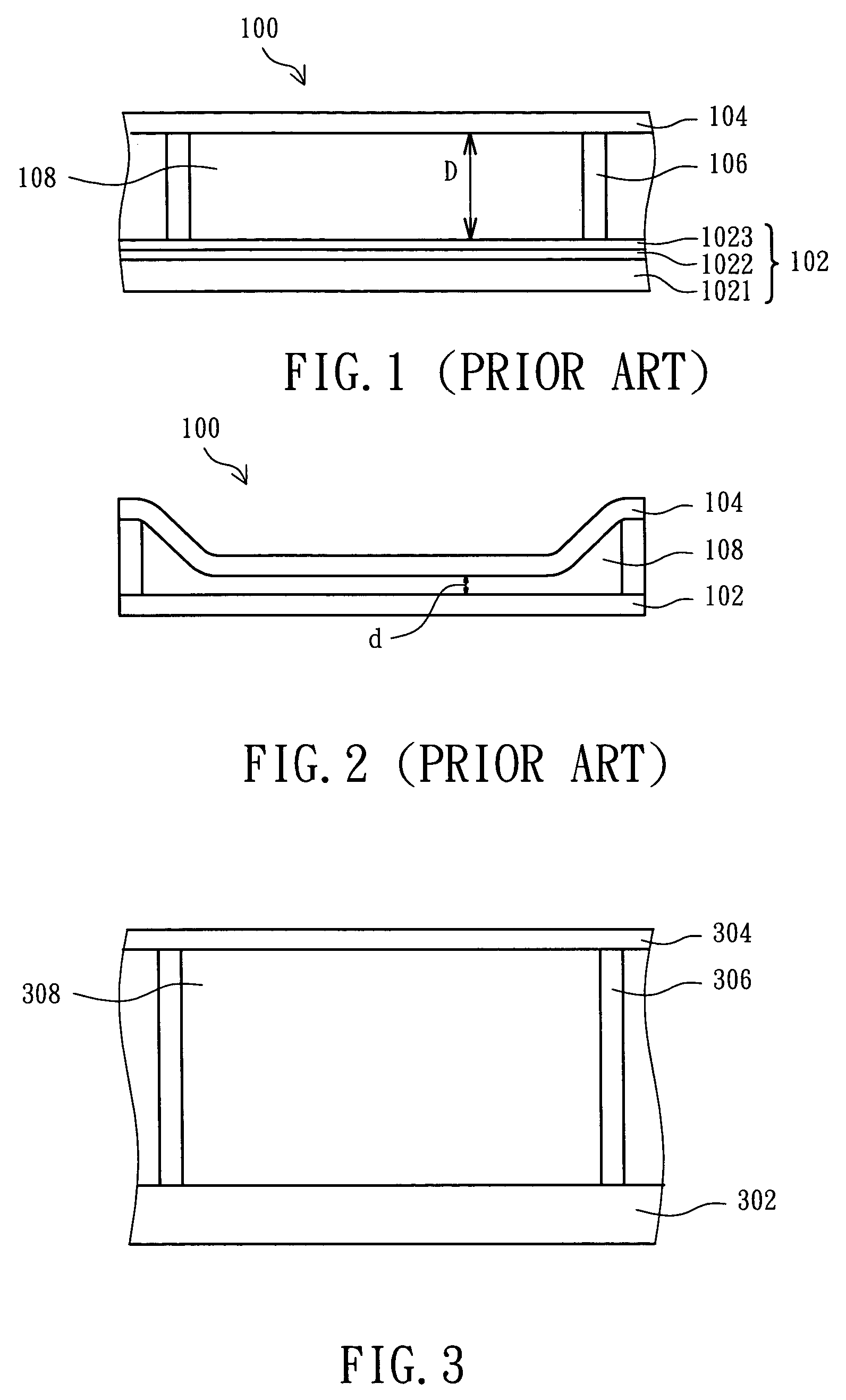
[0027] Please refer to FIG. 3. FIG. 3 shows a cross-section view of the modulation disclosed in the present invention. The modulation 303 comprises at least a light-incidence electrode 302 and a light reflection electrode 304. The light incidence electrode 302 and the light reflection electrode 304 are settled in parallel. These two electrodes are supported by posts 308, and a cavity 310 is then formed. The light incidence electrode 302 and the light reflection electrode 304 are selected from the group consisting of narrowband mirror, broadband mirror, non-metal mirror, metal mirror and the combination thereof.
[0028] Referring is made to FIG. 4, FIG. 4 shows a cross-section view of the light-incidence electrode of the modulation disclosed in the first embodiment of the present invention. Light-incidence electrode 302 is a semi-transparent electrode which comprises a substrate 3021 and a dielectric layer 3022. When the incident light goes through light-incidence electrode 302, part o...
embodiment 2
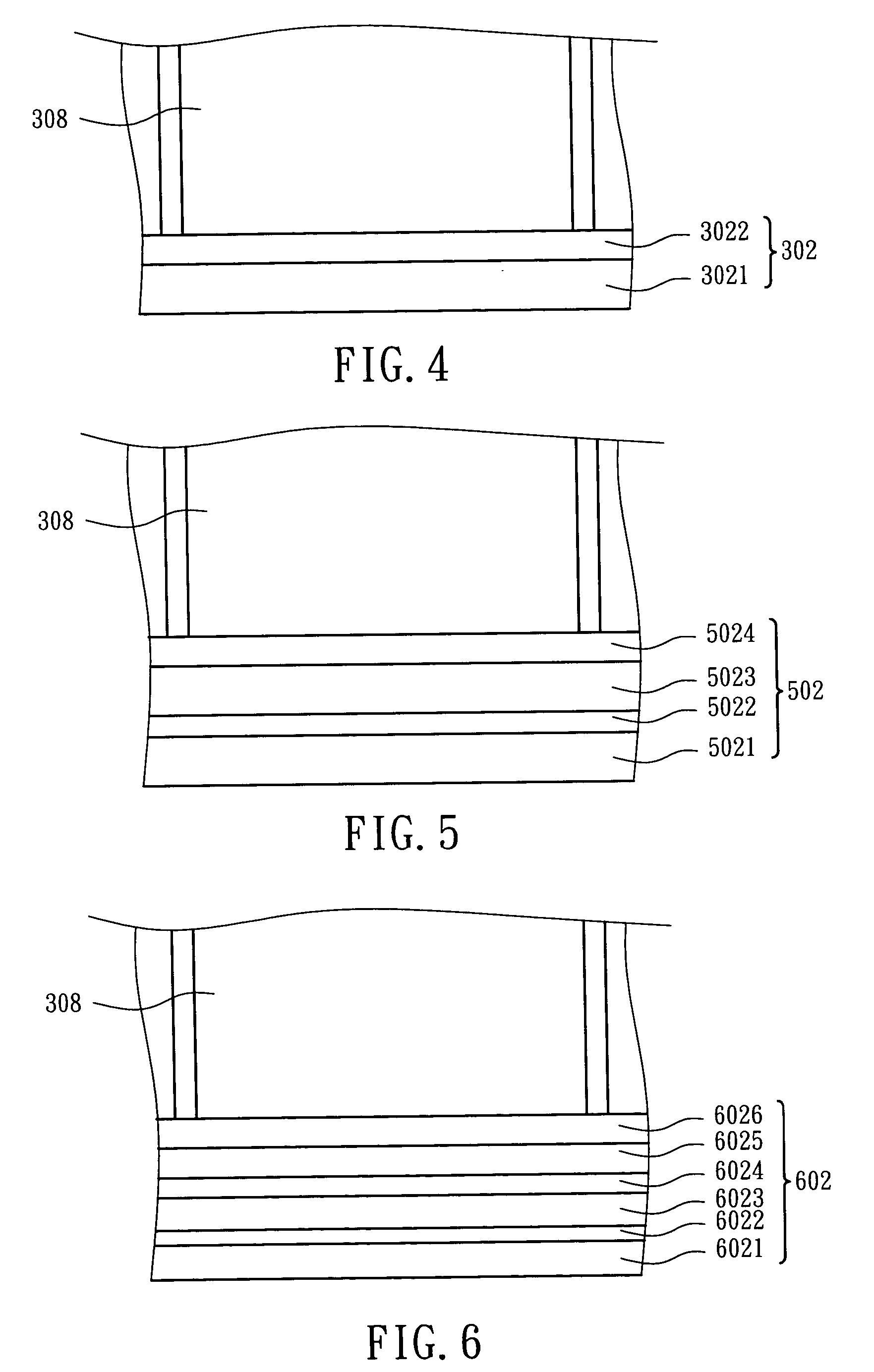
[0030] Referring is made to FIG. 5, FIG. 5 shows a cross-section view of the light incidence electrode of the modulation disclosed in the second embodiment. Similar to light incidence electrode 302 of modulation 300 in FIG. 3, light incidence electrode 502 comprises a substrate 5021, one first dielectric layer 5022, one conductive transparent layer 5023 and one second dielectric layer 5024. Incident light going through light incidence electrode 502 is partially absorbed. The substrate 5021 and the conductive transparent layer 5023 are made from a conductive transparent material, such as ITO, IZO, ZO and IO. The dielectric layer 5022 is made from silicon oxide, silicon nitrite or metal oxide.
[0031] The substrate 5021 and the conductive transparent layer 5023 function as an absorption layer. However, the substrate is formed on a glass plate (not shown in the figure) and the conductive transparent layer is formed on the top of the dielectric layer 5022. The lattice is disordered and th...
embodiment 3
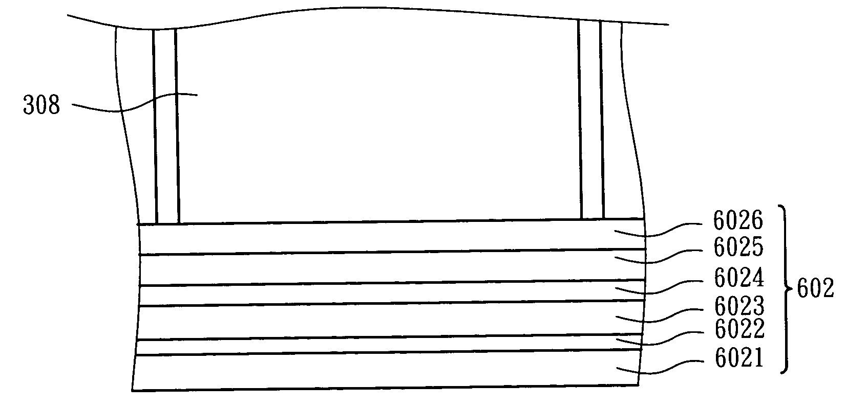
[0033] Please refer to FIG. 6. FIG. 6 shows the cross-section view of the modulation disclosed in the third embodiment of the present invention. As light incidence electrode 302 of modulation 300, the light incidence electrode 602 is a semi-transparent electrode which comprises a substrate 6021, one first dielectric layer 6022, one first conductive transparent layer 6023, one second dielectric layer 6024, one second conductive transparent layer 6025 and one third dielectric layer 6026. When the incident light goes through light-incidence electrode 602, part of the light is absorbed. Substrate 6021 and the two conductive transparent layers 6023 and 6025 are made from a conductive transparent material, for example, ITO, IZO, ZO, IO and the combination thereof. The material for forming dielectric layer 6022 is silicon oxide, silicon nitride or metal oxide.
[0034] Substrate 6021, the first conductive transparent layer 6023 and the second conductive transparent layer 6025 function as an a...
PUM
| Property | Measurement | Unit |
|---|---|---|
| conductive transparent | aaaaa | aaaaa |
| conductive transparent | aaaaa | aaaaa |
| conductive transparent | aaaaa | aaaaa |
Abstract
Description
Claims
Application Information