Developing device and process cartridge for an image forming apparatus

a development device and development cartridge technology, applied in the field of development devices and process cartridges for image forming apparatuses, can solve the problems of heavy stress on the developer, unstable amount of charge to be deposited on the toner grains, and toner electrostatically deposited

Inactive Publication Date: 2004-09-30
RICOH KK
View PDF20 Cites 15 Cited by
  • Summary
  • Abstract
  • Description
  • Claims
  • Application Information

AI Technical Summary

Benefits of technology

[0033] It is a second object of the present invention to provide toner that does not adhere to carrier grains included in a developer and prevents coating resin thereof from being shaved off.
[0034] It is a third object of the present invention to provide a developing device capable of maintaining the chargeability of the above toner stable over a long period of time to thereby obviate background fog and toner scattering against aging, a process cartridge including the same, and an image forming apparatus using the same.
[0035] It is a fourth object of the present invention to provide an image forming apparatus capable of maintaining the coating condition of a developer present on a developer carrier optimum before the developer enters a developing zone to thereby optimizing the density of the developer or magnet brush in the developing zone, thereby enhancing the durability of the dot image of a halftone portion and insuring an image with low granularity and high tonality.
[0036] It is a fifth object of the present invention to provide an image forming apparatus capable of controlling, while maintaining the coating condition of a developer present on a developer carrier optimum before the developer enters a developing zone, adequately controlling the amount of the developer to pass through the developing zone to thereby improving the durability of the developer and the stability of toner charging.

Problems solved by technology

When the developer is frictionally charged in the developing device due to agitation, the resulting electrostatic charge causes the toner to electrostatically deposit on the carrier.
However, the problem with the developer is that heavy stresses acts on the developer due to a long time of mixing and agitation and the presence of the doctor.
The stresses cause the additive to part from the toner grains or be buried in the same and bring about the separation of carrier coating layers as well as toner spent, rendering the amount of charge to deposit on the toner grains unstable and reducing the durability of the entire developer.
More specifically, the inorganic fine grains of silica, titanium oxide or similar additive deposited on the toner grains are susceptible to mechanical and thermal stresses and therefore apt to part from the toner grains or be buried in the same due to repeated agitation in the developing device.
However, in the case where the amount of the developer is reduced, it is necessary to reduce the amount of the developer not deposited on the sleeve because the developer must be present in the developing zone in a constant amount at all times. In this case, therefore, most part of the developer is deposited on and conveyed by the sleeve at all times and, as a consequence, subject to heavier stress ascribable to the doctor.
This requirement cannot be met unless the linear velocities of the photoconductive element and sleeve and developer conveying speed are increased, aggravating stresses to act on the developer.
On the other hand, the life of the developing device is determined mainly by the deterioration of the developer, particularly a decrease in the charging ability of the carrier ascribable to repeated development.
As a result, the overall amount of charge of the toner grains decreases and brings about toner scattering, background fog and other defects.
Further, the developing device is sophisticated in configuration and therefore high cost.
The magnet roller, however, increases the amount of the developer, which stays at the position upstream of the doctor, more than when the magnet roller is absent, so that more developer is subject to stress by being held in a developer layer upstream of the doctor.
Further, it is likely that stress to act on the individual developer grains increases.
Although this method reduces a frictional force and other stresses to act on the developer, toner contained in the developer cannot be sufficiently charged and therefore fails to form a satisfactory image.
However, considering the current trend toward a lower melting point and a smaller grain size of a toner material that aggravate the adhesion of toner components to carrier surfaces, the prior art schemes described above are not satisfactory in the aspect of a margin as to the adhesion of toner components to carrier surfaces.
It is therefore difficult to obviate background fog, toner scattering and other problems, which are ascribable to a decrease in the amount of charge due to aging and lower image quality.
The alternating electric field, however, brings about discharge due to a local increase in electric field ascribable to the irregular density of the magnet brush in the developing region, particularly in deep portions of a latent image, causing an image to be lost in the form of a ring.
Therefore, the resistance of the carrier for development is limited, i.e., it is difficult to use a carrier with low resistance.
Furthermore, even when a carrier with medium or high resistance is used, local breakdown ascribable to irregular coating layers occurs and also brings about discharge.
In this respect, even the uniformly of carrier coating layers and the resistance of the carrier cores, i.e., the material of the cores are limited.
Further, if the slip efficiency and therefore the amount of the developer in the developing zone is excessively increased, then the developer is packed in the upstream and center portions of the developing zone.
As a result, a magnet brush rises in the upstream portion and obstructs development that should originally be effected when the magnet brush contacts the photoconductive element.
Also, the developer packed in the center portion scrapes off toner grains present on the photoconductive element by scavenging, lowering developing efficiency in the developing zone.
Laid-Open Publication Nos. 7-121031 and 7-128982 also mentioned earlier have a problem that the density of the developer or that of the magnet brush in the actual developing zone is determined by a gap for development, the curvature of the photoconductive element and that of the sleeve, i.e., the density of the magnet brush measured on a developing roller differs from the actual system.
Such stress, acting on the developer layer X, brings about various problems stated previously.
This brings about a problem that when the fluidity or the bulk density of the developer varies due to repeated operation, the amount of the developer to move toward the sleeve is apt to become unstable, requiring the gap between the screw and the sleeve to be reduced or the volume of the developer itself to be increased.
However, this kind of scheme is apt to aggravate irregularity in the amount of the developer upstream of the doctor pole.
Moreover, the decrease in the amount of the developer to reach the developing zone becomes noticeable after repeated operation, making image quality unstable.
In addition, the charging of the toner is obstructed at the doctor due to a short conveying force.

Method used


Image

  • Developing device and process cartridge for an image forming apparatus
  • Developing device and process cartridge for an image forming apparatus
  • Developing device and process cartridge for an image forming apparatus

Examples


experiment 2

[0116] [Experiment 2]

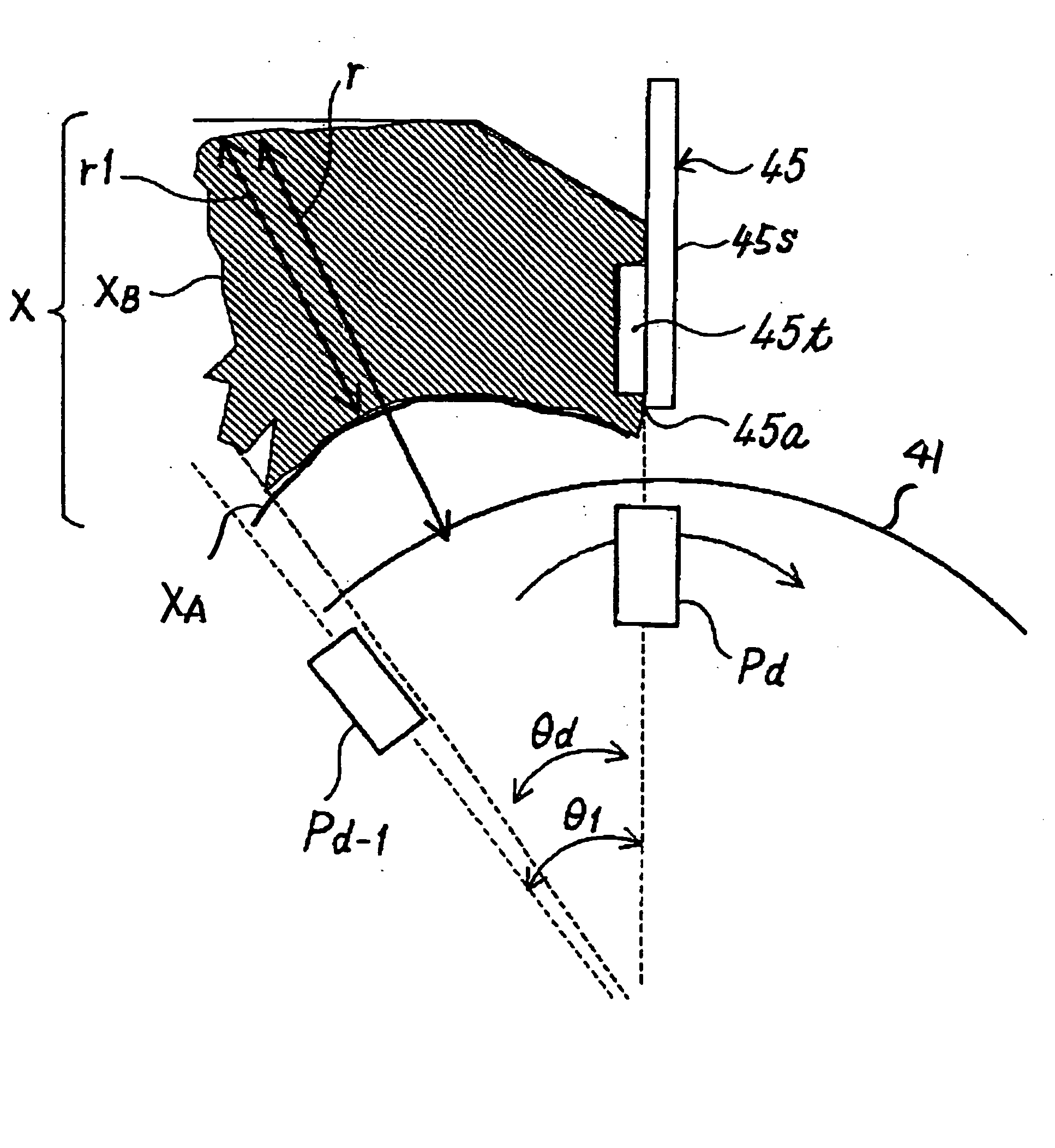
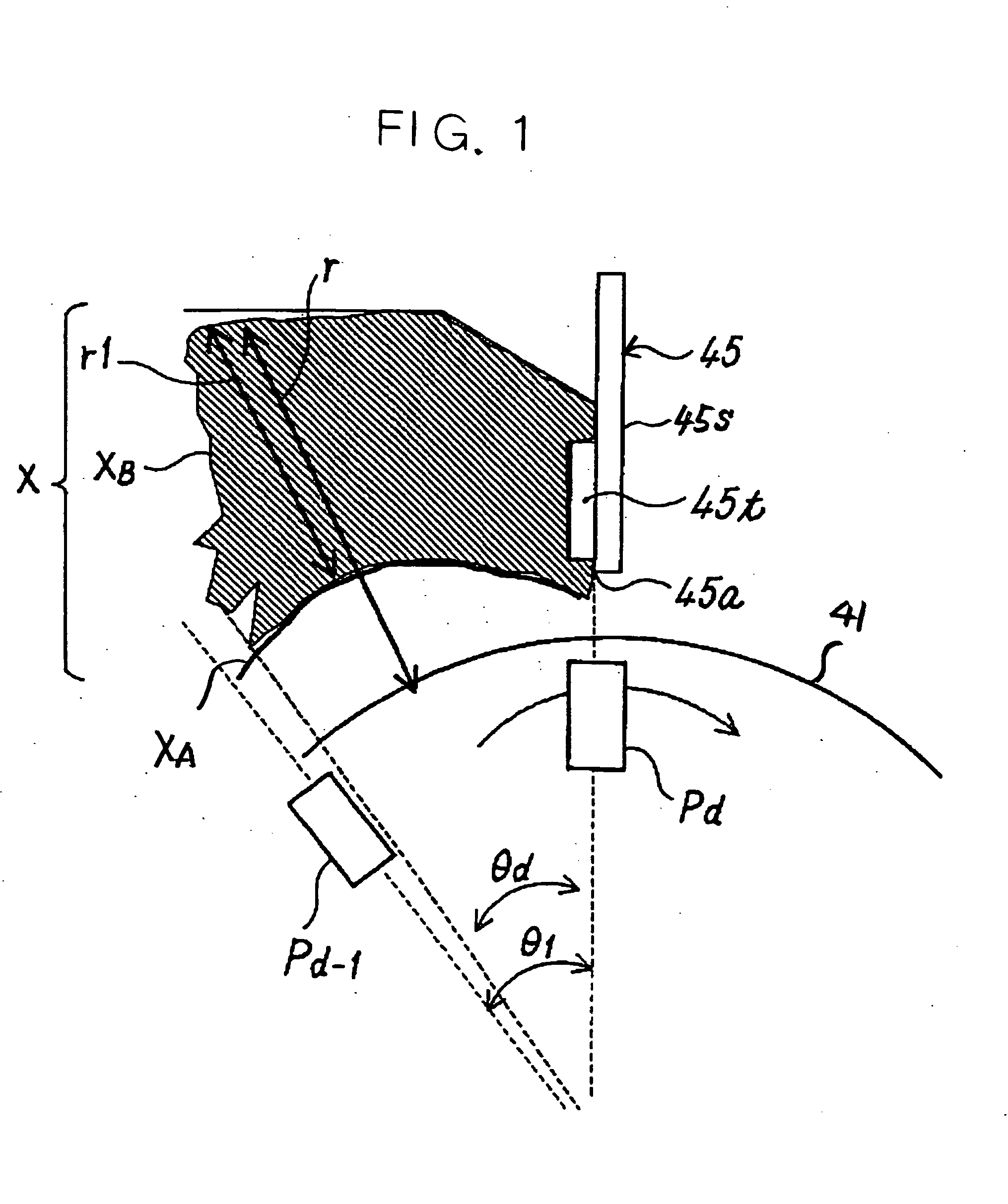
[0117] The thickness of the stationary layer XB in the radial direction of the sleeve was varied in each of the conventional printer and illustrative embodiment in order to determine how the carrier charging ability CA varied in accordance with the number of sheets output. Experiment 2 differs from Experiment 1 in that the thickness of the stationary layer XB was varied by varying the clearance or distance between the sleeve and the casing C of the developing device.

[0118] FIGS. 12A and 12B each show a particular condition of the stationary layer XB dependent on the clearance between the sleeve 2 and the casing C (casing clearance hereinafter). As shown in FIG. 12A, when the casing C is gently inclined relative to the surface of the sleeve 2 upstream of the doctor 45 such that it leaves the above surface little by little over a substantial distance, the stationary layer XB is thin. By contrast, as shown in FIG. 12B, when the casing C is sharply inclined relative...

second embodiment

[0140] This embodiment is directed toward the second and third objects stated earlier. Reference will be made to FIGS. 15 and 16 for describing an electrophotographic image forming apparatus and a developing device included in the same and using a two-ingredient type developer.

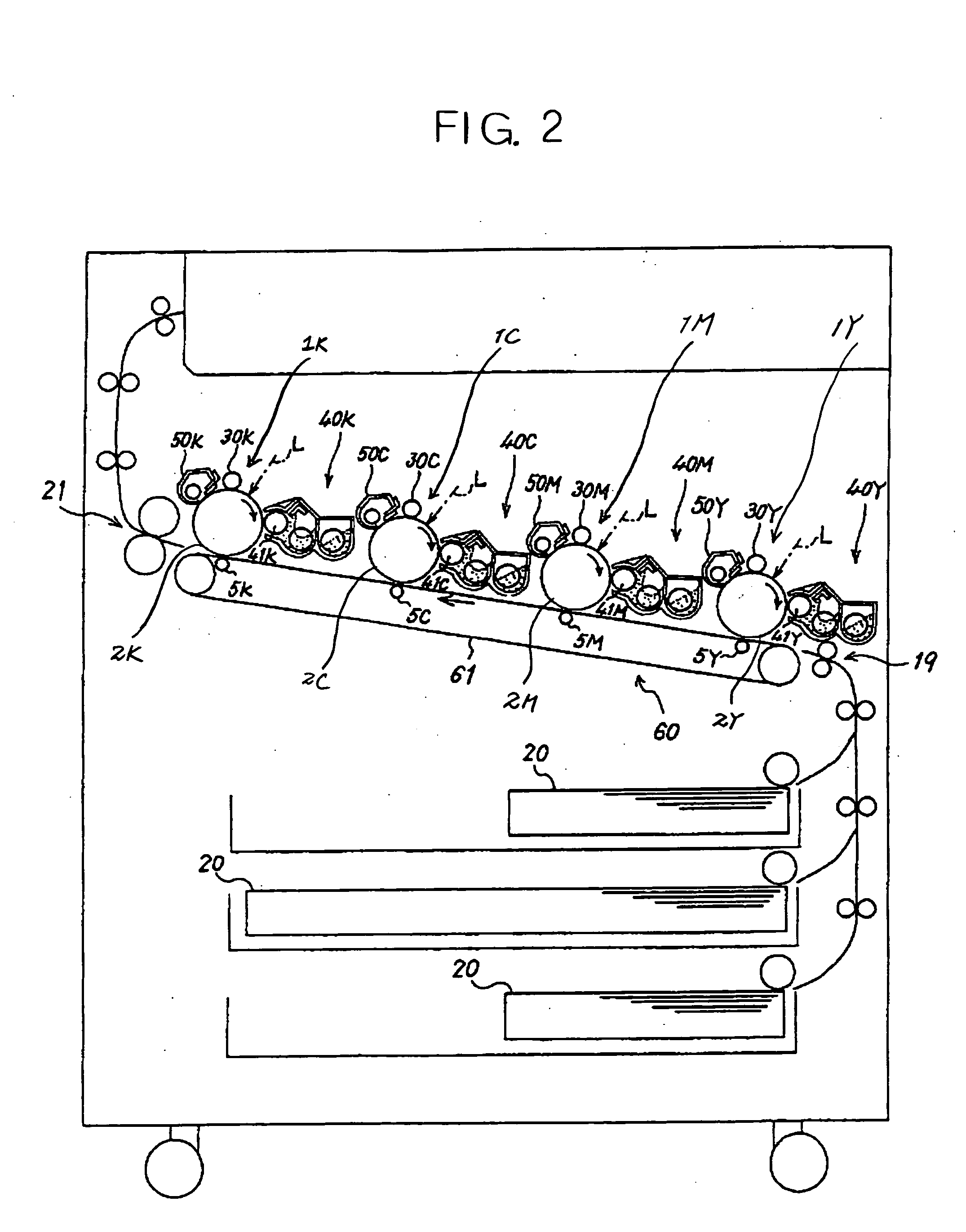
[0141] As shown in FIG. 15, the image forming apparatus includes a charger 30, an exposing unit represented by a laser beam L, a developing device 40, an image transferring device 5 and a cleaning device 50, which are arranged around a photoconductive drum or image carrier 2. A fixing unit 21 fixes a toner image transferred to a sheet or recording medium by the image transferring device 5.

[0142] The drum 2, made up of a hollow core and a photoconductor coated on the core, is caused to rotate in a direction indicated by an arrow in FIG. 15 by a drive mechanism not shown. After the charger 30 has uniformly charged the surface of the drum 2 to a preselected potential, the laser beam L scans the charged surface of...

third embodiment

[0179] This embodiment is directed toward the fourth and fifth objects stated earlier. A developing method unique to the illustrative embodiment will be described first. As for the configuration and operation of a developing device, this embodiment is essentially identical with the first embodiment described with reference to FIGS. 2 through 4 and will therefore be described with reference also made to FIGS. 2 through 4, as needed.

[0180] FIG. 19 shows the condition of a two-component type developer being conveyed via a developing zone in accordance with the illustrative embodiment. FIG. 20 shows the condition of FIG. 19 in the developing zone, as seen from the drum 2 side. The sleeve 41 accommodates the magnet roller not shown, as stated earlier. Labeled C and D are respectively a developing zone and a zone where an apparent coating ratio is measured. The developing zone C refers to a zone where a magnet brush, i.e., brush chains formed by carrier grains contact the drum 1 and cause...


PUM


Abstract

A developing device of the present invention includes stationary layer angle setting means. Assume that a developer layer, staying at a position upstream of a metering member in a direction in which a developer carrier conveys a developer, consists of a stationary layer in which the developer is not replaced and a flowing layer in which it is replaced, that an angle between, as seen from the axis of the developer carrier, the upstream edge portion, in the above direction, of the end portion of the metering member, which faces the developer carrier, and a position where the end of the stationary layer upstream of, but remote from the edge portion, is located is thetad, and that an angle between, as seen from the above axis, the edge portion and a position where a magnetic pole is positioned just upstream of a doctor pole in the above direction is theta1. Then, the angle thetad lies in a preselected range relative to the angle theta1.

Description

[0001] 1. Field of the Invention[0002] The present invention relates to a copier, printer, facsimile apparatus or similar image forming apparatus and more particularly to a developing device for forming an image with a two-ingredient type developer made up of toner grains and magnetic carrier grains and a process cartridge including the same.[0003] 2. Description of the Background Art[0004] It is a common practice with an image forming apparatus to form a toner image by using a photoconductive element or image carrier provided with a photoconductive layer on its surface and a developing device. A two-ingredient type developer, made up of a toner and a magnetic carrier, is extensively applied to the developing device because it is feasible for color image formation. When the developer is frictionally charged in the developing device due to agitation, the resulting electrostatic charge causes the toner to electrostatically deposit on the carrier. The carrier, thus supporting the toner...

Claims


Application Information

Patent Timeline
Patent Type & Authority Applications(United States)
IPC IPC(8): G03G15/09
CPCG03G2215/0634G03G15/09
Inventor TAKEUCHI, NOBUTAKAOYAMA, HAJIMETAKAGAKI, HIROMITSUKOIKE, TAKAYUKI
Owner RICOH KK
Why Eureka
Try Eureka