

Method for manufacturing semiconductor chip
- Summary
- Abstract
- Description
- Claims
- Application Information
AI Technical Summary
Benefits of technology
Problems solved by technology
Method used
Image

Examples
Embodiment Construction
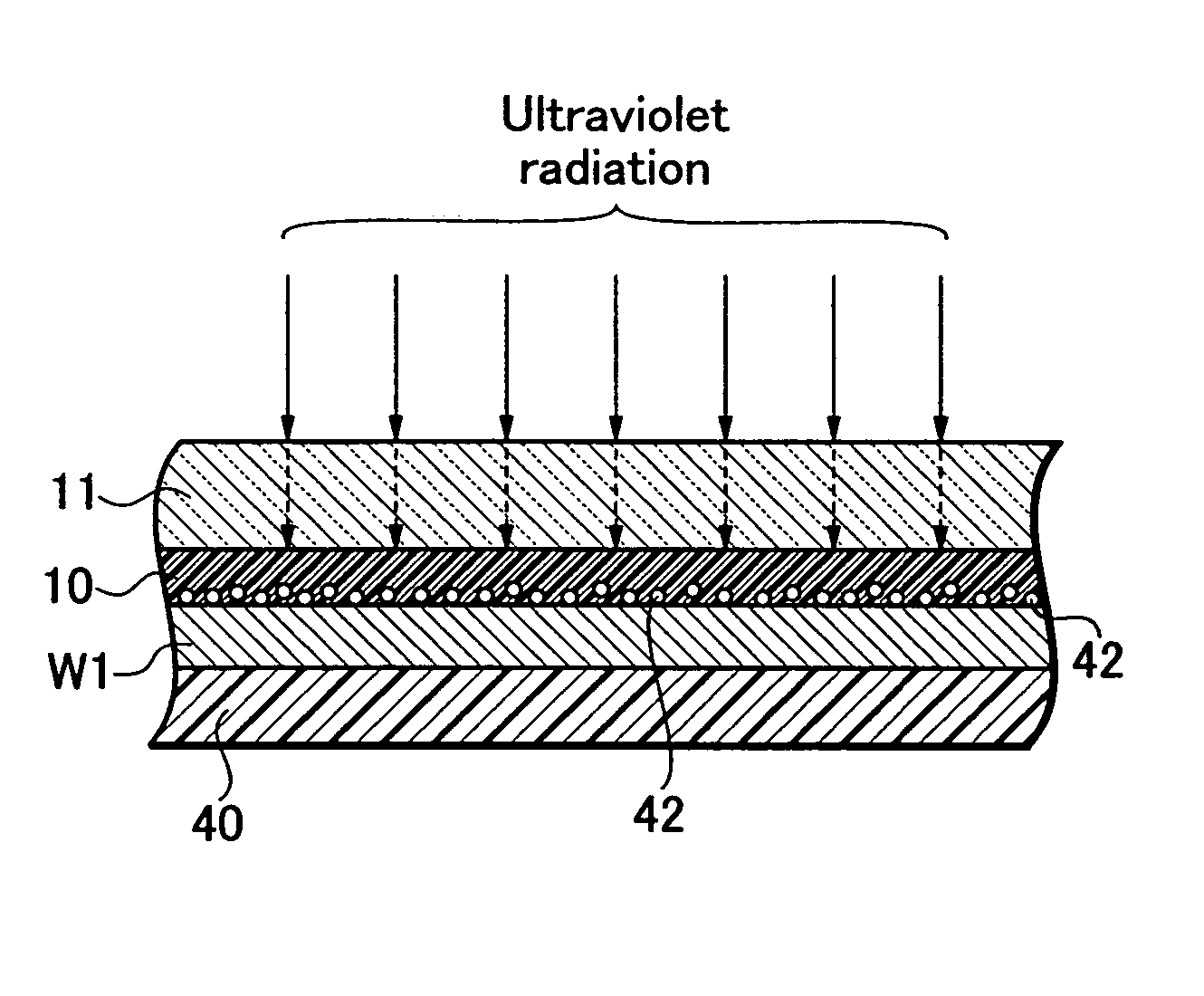
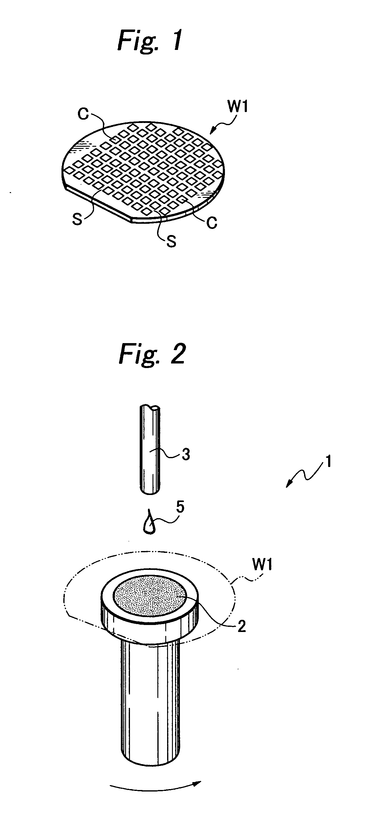
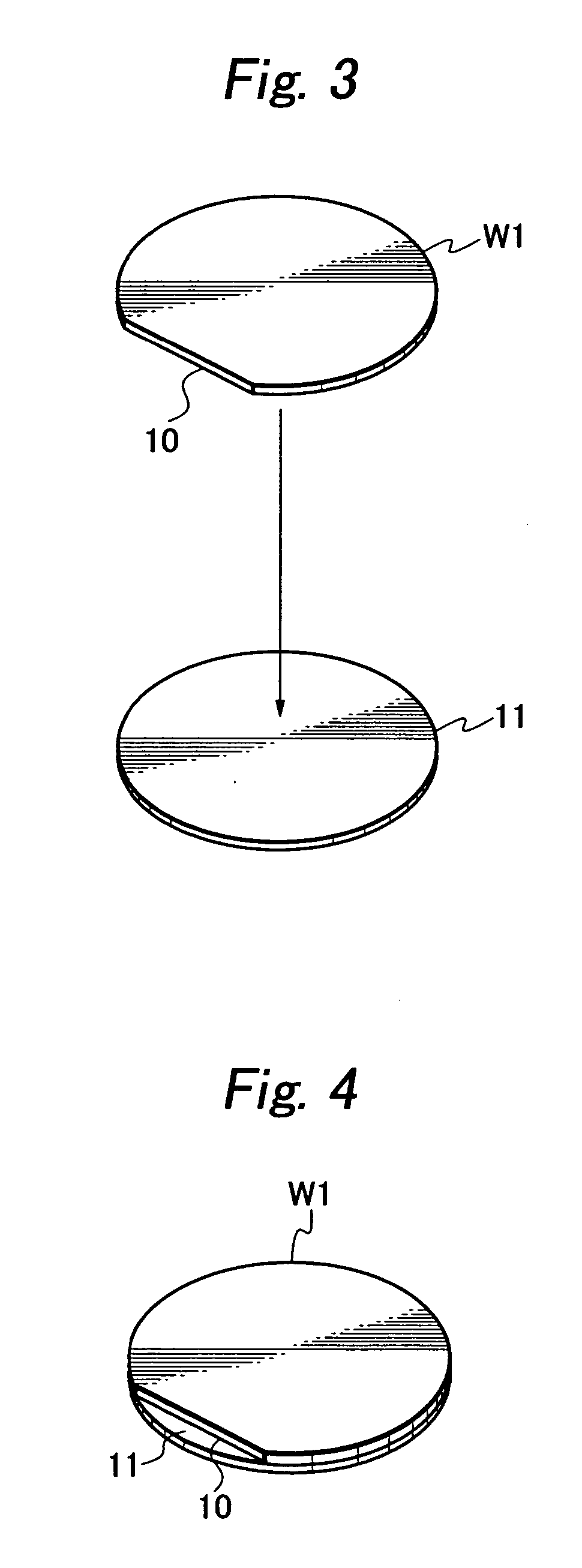
[0044] As an embodiment of the present invention, explanation is made on a method that the semiconductor wafer W1, segmented by streets S and formed with a plurality of circuits C, is divided into individual semiconductor chips, as shown in FIG. 1.
[0045] At first, a spin coater 1, for example, shown in FIG. 2 is used, to coat an adhesive layer having an adhesion force to reduce upon exposed to light, e.g. liquid resin 10, over the surface of a semiconductor wafer W1 or support substrate 11. The explanation herein is on a case that liquid resin 10 is coated to the surface of the semiconductor wafer W1.
[0046] The spin coater 1 has at least a rotatable support table 2 and a drip part 3 for allowing liquid resin 10 to drip. The semiconductor wafer W1 is held face up on the support table 2. While the support table 2 is rotated at a rotation speed, for example, of 100-8000 rpm for 5 seconds or more, liquid resin is allowed to drip through the drip part 3, to carry out spin coating. Due to...
PUM
 Abstract
Description
Claims
Application Information