Methods for substrate orientation

a substrate orientation and substrate technology, applied in the direction of photomechanical equipment, instruments, originals for photomechanical treatment, etc., can solve the problems of loss of critical dimensions of features, undercut phenomenon of metal layer below the patterned resist, and less than desirable patterning of the photomask in subsequent photolithographic processes

Inactive Publication Date: 2004-10-21
APPLIED MATERIALS INC
View PDF49 Cites 384 Cited by
  • Summary
  • Abstract
  • Description
  • Claims
  • Application Information

AI Technical Summary

Problems solved by technology

Conventional etching processes, such as wet etching, tend to etch isotropically, which can result in an undercut phenomenon in the metal layer below the patterned resist.
The undercut phenomenon can produce patterned features on the photomask that are not uniformly spaced and do not have desired straight, vertical sidewalls that are necessary to produce the critical dimensions of the features.
Additionally, the isotropic etching of the features may overetch the sidewalls of features in high aspect ratios, resulting in the loss of the critical dimensions of the features.
Features formed without the desired critical dimensions in the metal layer can detrimentally affect light passing therethrough and result in less than desirable patterning by the photomask in subsequent photolithographic processes.
However, it has been observed that dry etching of the reticles, which are generally square in shape, may provide variable or non-uniform etching of similar features disposed in the metal layer and located at different locations on the reticle surface.
It is believed that one factor that arises in this substrate or global non-uniformity of etching features is due to the asymmetry of dry etching process chambers.
However, redesigning chambers is a costly and time consuming process of trial and error to remove or minimize process variations.

Method used


Image

  • Methods for substrate orientation
  • Methods for substrate orientation
  • Methods for substrate orientation

Examples


Embodiment Construction

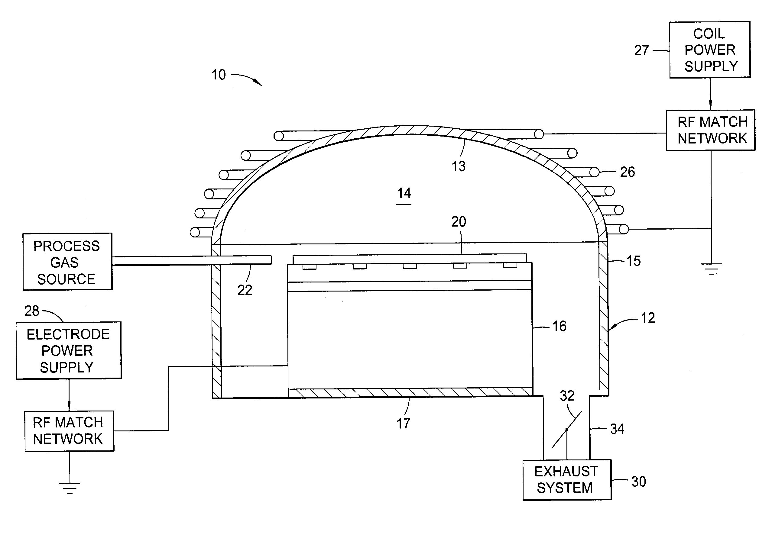
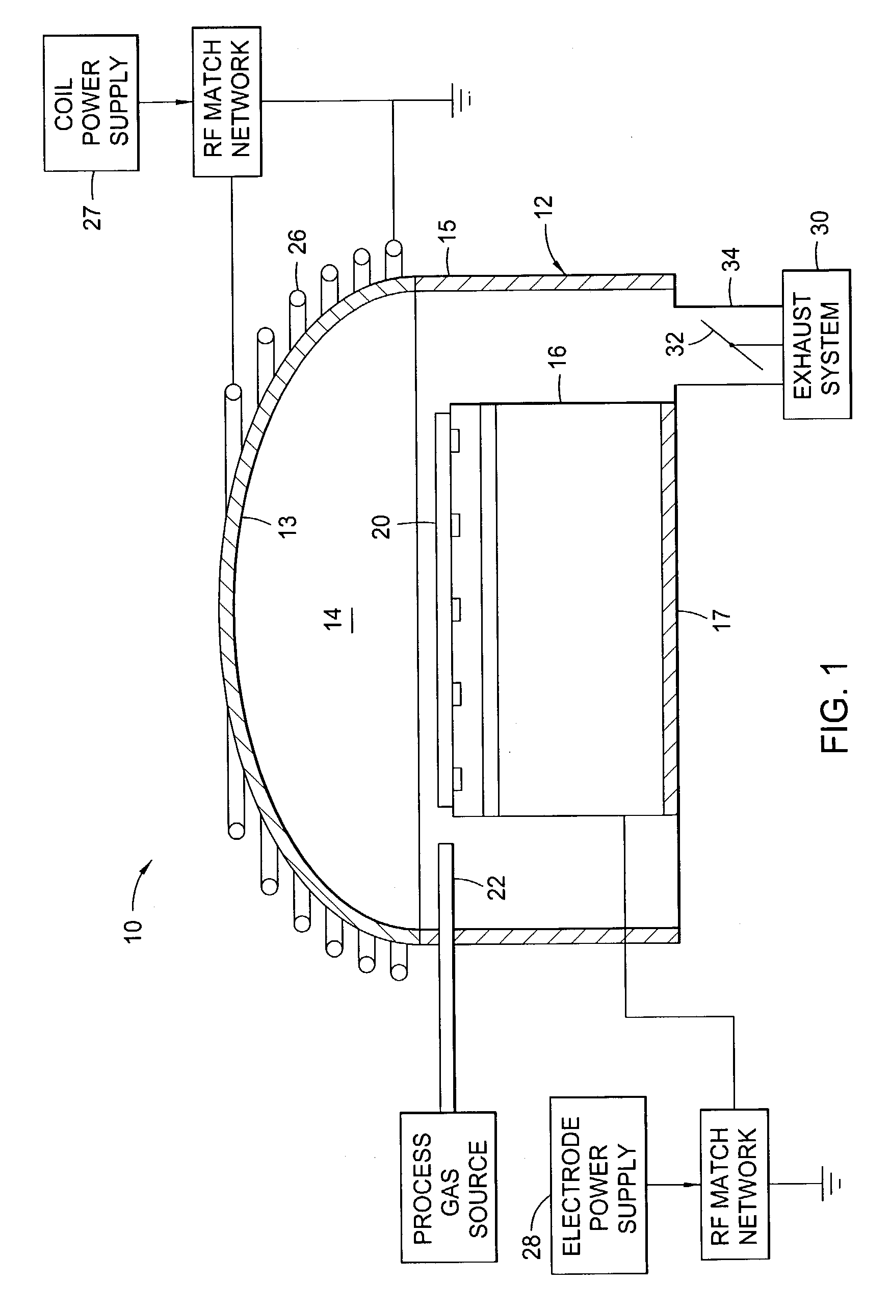
[0022] Aspects of the invention will be described below in reference to an inductively coupled plasma etch chamber. Suitable inductively coupled plasma etch chambers include the Tetra.TM. photomask etch chambers available from ETEC of Hayward, Calif., or optionally, the Decoupled Plasma Source (DPS.TM.) chamber available from Applied Materials, Inc., of Santa Clara, Calif. Other process chambers may be used to perform the processes of the invention, including, for example, capacitively coupled parallel plate chambers and magnetically enhanced ion etch chambers as well as inductively coupled plasma etch chambers of different designs. Although the processes are advantageously performed with the ETEC Tetra.TM. photomask etch chamber, the description in conjunction with the DPS.TM. processing chamber is illustrative, and should not be construed or interpreted to limit the scope of aspects of the invention.

[0023] FIG. 1 is a schematic cross-sectional view of one embodiment of a processin...


PUM

PropertyMeasurementUnit
poweraaaaaaaaaa
poweraaaaaaaaaa
bias poweraaaaaaaaaa

Abstract

Method and apparatus for etching a metal layer disposed on a substrate, such as a photolithographic reticle, are provided. In one aspect, a method is provided for processing a photolithographic reticle including positioning the reticle in a first orientation on a reticle support in a processing chamber, wherein the reticle comprises a metal photomask layer formed on an optically transparent substrate, and a patterned resist material deposited on the metal photomask layer, etching the metal photomask layer in the first orientation, positioning the reticle in at least a second orientation, and etching the metal photomask layer in the at least second orientation.

Description

[0001] 1. Field of the Invention[0002] The present invention relates to the fabrication of integrated circuits and to the fabrication of photolithographic reticles useful in the manufacture of integrated circuits.[0003] 2. Background of the Related Art[0004] Semiconductor device geometries have dramatically decreased in size since such devices were first introduced several decades ago. Since then, integrated circuits have generally followed the two year / half-size rule (often called Moore's Law), which means that the number of devices on a chip doubles every two years. Today's fabrication plants are routinely producing devices having 0.15 .mu.m and even 0.13 .mu.m feature sizes, and tomorrow's plants soon will be producing devices having even smaller geometries.[0005] The increasing circuit densities have placed additional demands on processes used to fabricate semiconductor devices. For example, as circuit densities increase, the widths of vias, contacts and other features, as well ...

Claims


Application Information

Patent Timeline
Patent Type & Authority Applications(United States)
IPC IPC(8): C23F4/00G03F1/80H01L21/302H01L21/461
CPCC23F4/00G03F1/80H01J37/321
Inventor BUXBAUM, ALEXSKYBERG, BJORN
Owner APPLIED MATERIALS INC
Why Eureka
Try Eureka