Method and arrangement for aligning an optical component on a printed wiring board

a technology of printed wiring boards and optical components, applied in the direction of optical elements, circuit optical details, instruments, etc., can solve the problems of providing defective printed circuit board structures, no fast automatic way for aligning active optical components, and known slight misalignments

Inactive Publication Date: 2004-12-30
MOTOROLA INC
View PDF7 Cites 3 Cited by
  • Summary
  • Abstract
  • Description
  • Claims
  • Application Information

AI Technical Summary

Problems solved by technology

One of the reasons for this is that there is no fast automatic way for aligning an active optical component to the electrical layout and to the laser light beam of the optical omponent.
However, slight misalignments are known to occur between the position of the solder mask on the one hand, and the fiducials and terminal pads on the pri

Method used


Image

  • Method and arrangement for aligning an optical component on a printed wiring board
  • Method and arrangement for aligning an optical component on a printed wiring board
  • Method and arrangement for aligning an optical component on a printed wiring board

Examples


Embodiment Construction

)

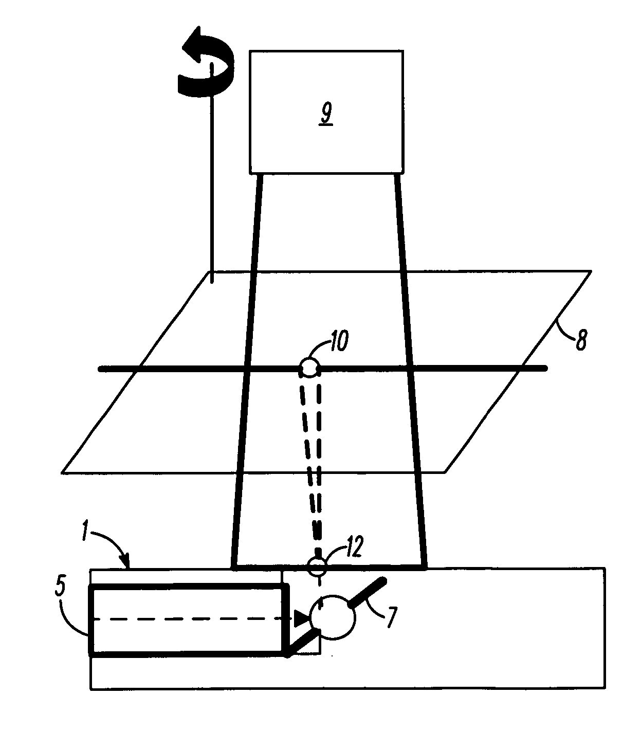
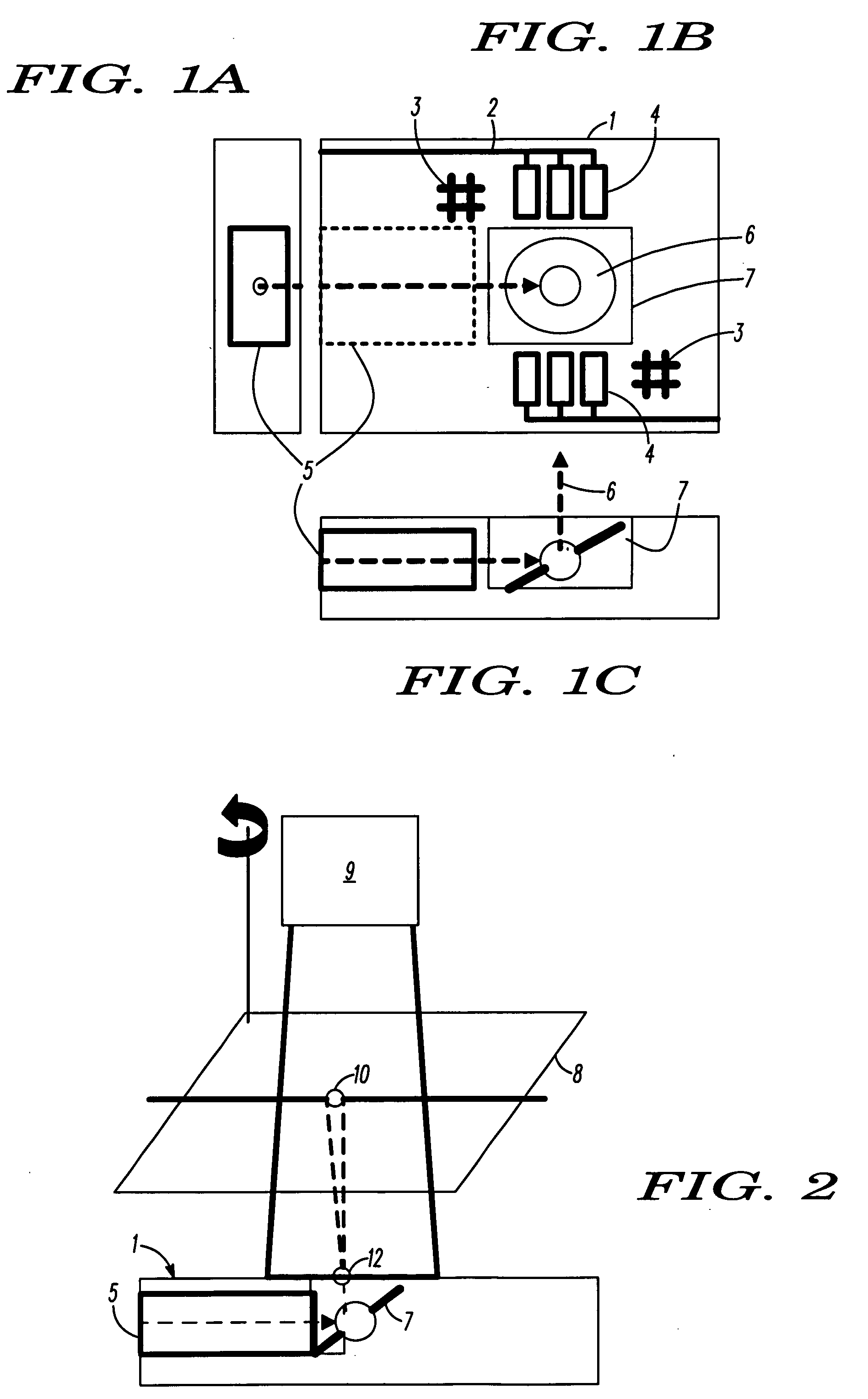
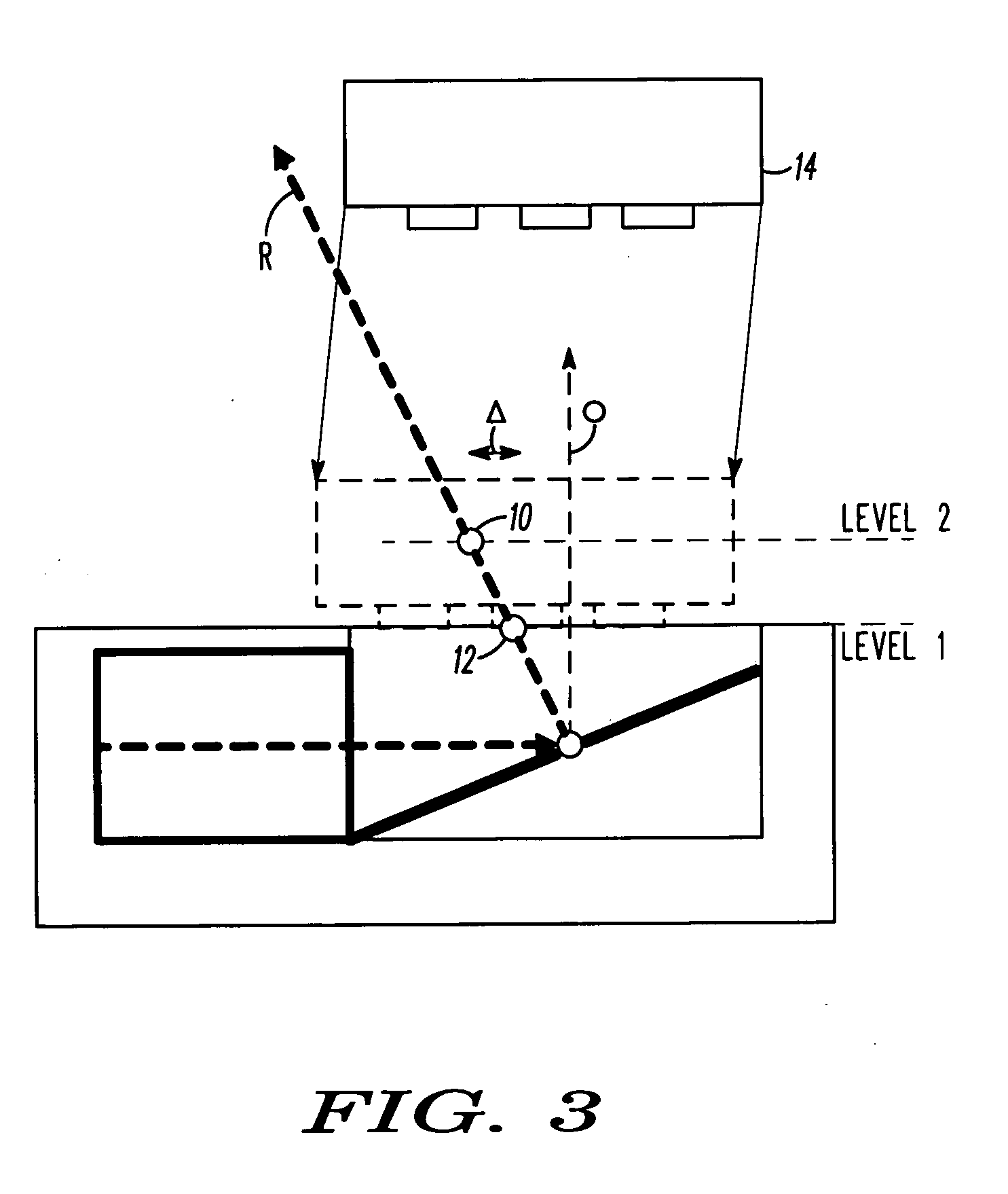
[0015] Referring firstly to FIG. 1, a PWB (1) has on its upper surface (hereafter referred to as level 1) an electrical layout made out of copper traces in conventional manner. This layout consists out of copper lines (2), pads (3) and a number of fiducials (4) of which two sets are shown. The PWB additionally has an underlying optical layer, which is built up out of embedded waveguides (5). Light beams (6) of different wavelength can run through this optical waveguide. To guide a light beam into an optical detector, which is to be mounted on the top of the PWB it is necessary to redirect the light beam using an embedded mirror (7). For assembly of the detector on the top of the PWB it is necessary to place the component exactly aligned to the electrical layout and to the light beam (6). A standard approach (for example, that described in the previously discussed U.S. Pat. No. 6,044,549) is used to align the detector component to the electrical layout of the PWB using the defined f...


PUM


Abstract

A method and arrangement for aligning an optical component (14) on a printed wiring board (1) by using a reflector (8) below a surface mount technology camera to determine the offset (Delta) between the printed wiring board electrical layout and the light beam in the printed wiring board optical layer. This provides the following advantages: Component alignment to optical layer and component alignment to mirror reflection in optical layer, Fast placement process for optical components, Flexible process because there is no need for component specific fixtures, and Compatible with standard SMT processes and standard SMT placement machines.

Description

[0001] This invention relates to opto / electronic assemblies.[0002] In the field of this invention it is known that assembly of optical components in opto / electronic arrangements is done manually or with slow semi-automatic machines. One of the reasons for this is that there is no fast automatic way for aligning an active optical component to the electrical layout and to the laser light beam of the optical omponent.[0003] From U.S. Pat. No. 6,044,549 there is known the manufacture of printed circuit board structures which include a substrate (i.e., a printed circuit board) and electronic components mounted upon the substrate for automatic assembly of the components onto the substrate; components need to be positioned substantially exactly in their required location to ensure the terminals on the components are aligned correctly with terminal pads on the substrate, to which they are to be soldered. For this purpose, registration datum positions are provided upon a substrate. The datum...

Claims


Application Information

Patent Timeline
IPC IPC(8): G02B6/42G02B6/43H05K1/02H05K13/04
CPCG02B6/4222G02B6/43H05K1/0274H05K13/0413H05K13/0812
Inventor SCHALLER, ANDREASMACHANDE, THORSTEN
Owner MOTOROLA INC
Why Eureka
Try Eureka