Apparatus and method for treating edge of substrate

Inactive Publication Date: 2005-01-06
SAMSUNG ELECTRONICS CO LTD
View PDF7 Cites 23 Cited by
  • Summary
  • Abstract
  • Description
  • Claims
  • Application Information

AI Technical Summary

Benefits of technology

[0008] In view of the foregoing, the present invention provides apparatus and met

Problems solved by technology

Unfortunately, such a conventional manner includes additional steps of shielding a pattern-formed portion by the shielding solution or the mask and re-removing the pattern-formed portion after etching.
This results in a substantial amount of lost work time and the use of a

Method used


Image

  • Apparatus and method for treating edge of substrate
  • Apparatus and method for treating edge of substrate
  • Apparatus and method for treating edge of substrate

Examples


Example

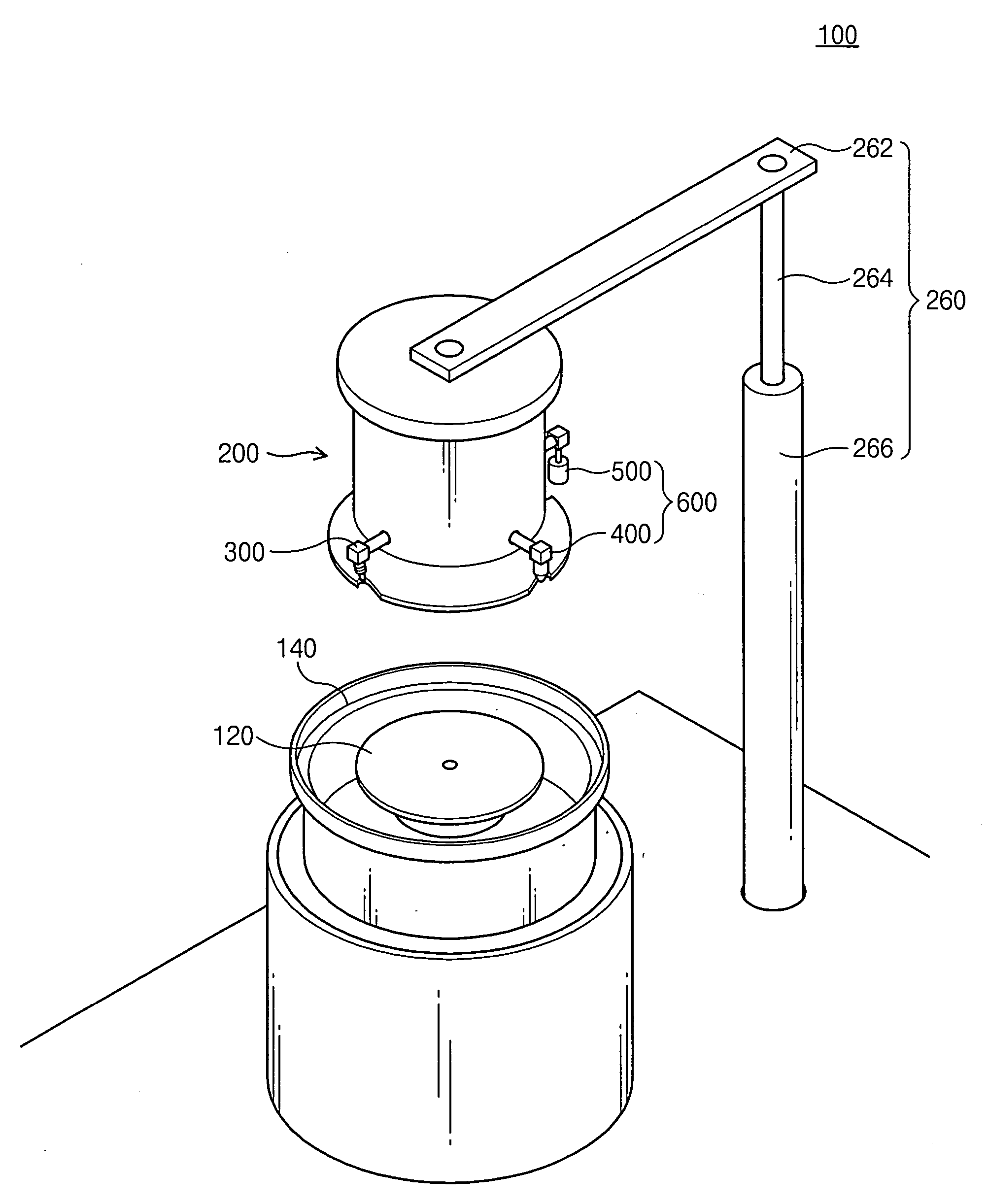
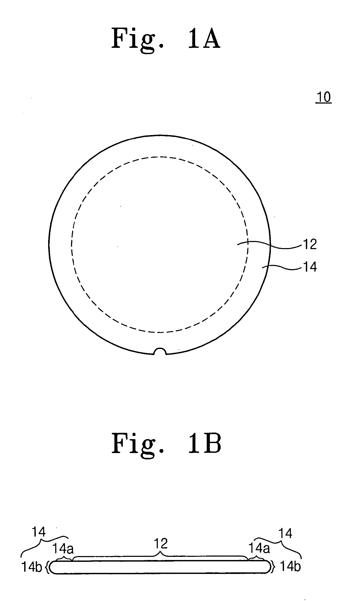
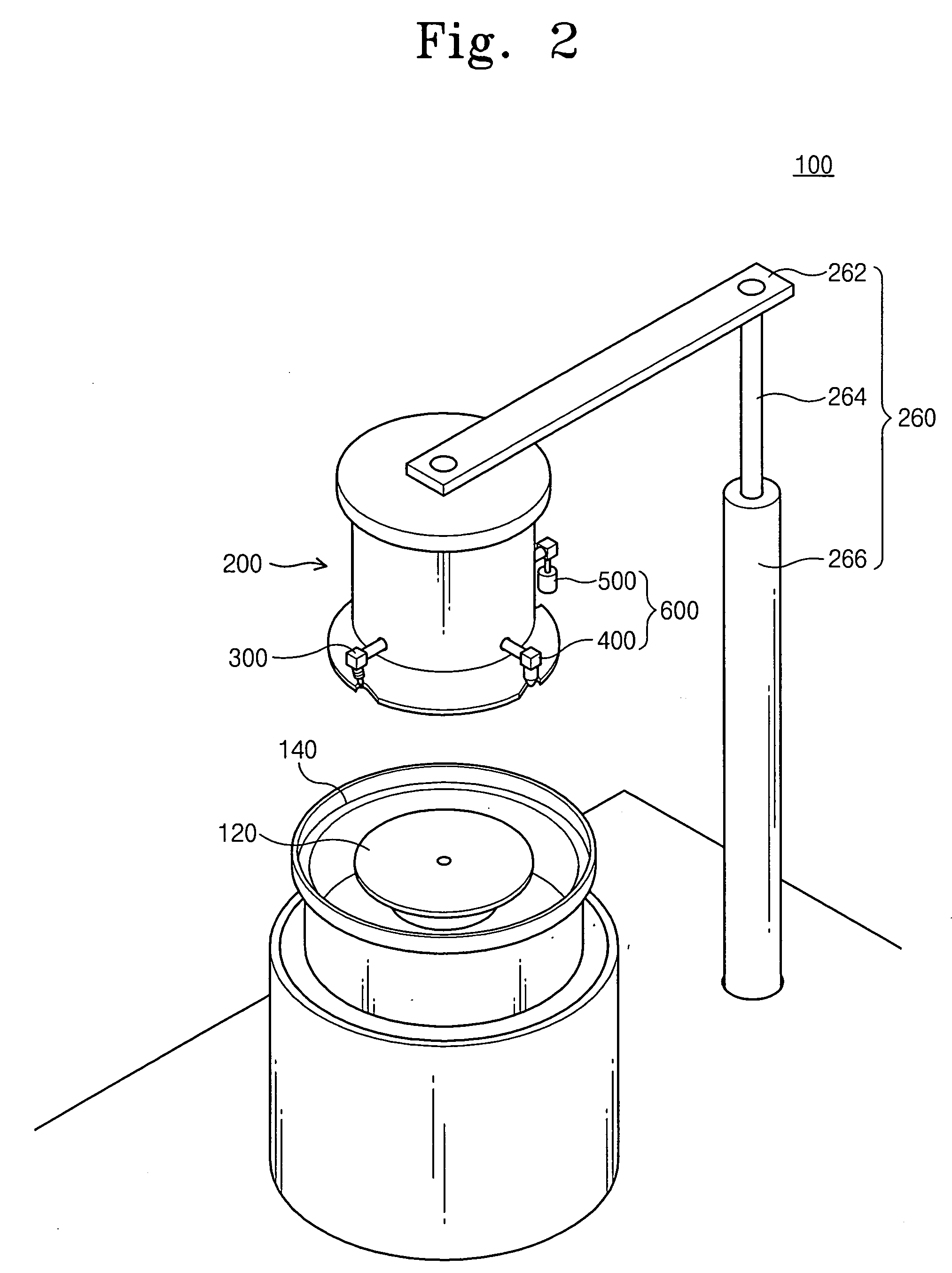
[0025] A wafer 10 will now be defined with reference to FIG. 1A and FIG. 1B. In this embodiment, a top surface of the wafer 10 is a surface on which a pattern is formed, and a bottom surface thereof means the other surface. Further, a shielding surface 12 of the wafer 10 means a surface within the confines of a wafer edge 14, in which incomplete chips are disposed. The shielding surface 12 is shielded from an etchant sprayed to the wafer edge 14. The wafer edge 14 comprises an upper edge 14a corresponding to a top surface edge of the wafer 10 and an edge bevel portion 14b corresponding to a portion protruding from a lateral side of the wafer 10.

[0026] Referring to FIG. 2, a semiconductor substrate edge treating apparatus 100 includes a susceptor 120, a shielding cover 200, an etchant spray part 300, and a cleaning device 600. The susceptor 120 may be a circular plate on which a wafer 10 is placed. The wafer 10 may be fixed to the susceptor 120 by means of a clamp which functions as...


PUM

PropertyMeasurementUnit
Semiconductor propertiesaaaaaaaaaa

Abstract

An apparatus for treating an edge of a semiconductor substrate includes an etchant supply nozzle for supplying a first etchant to the edge of the semiconductor substrate. The apparatus further includes a shielding cover for preventing an etchant from flowing to a shielding surface of the semiconductor substrate. The shielding cover is movable in an upward and downward direction. The apparatus also includes a device for cleaning the edge of the semiconductor substrate. According to the apparatus, after a wafer edge is etched, foreign substances remaining at the wafer edge is efficiently removed.

Description

[0001] This application claims the priority of Korean Patent Application No. 2003-44679, filed on Jul. 2, 2003 in the Korean Intellectual Property Office, the disclosure of which is incorporated herein in its entirety by reference. BACKGROUND OF THE INVENTION [0002] 1. Field of the Invention [0003] The present invention relates to apparatus and method for manufacturing semiconductor devices and, more particularly, to apparatus and method for removing and cleaning layers left at the edge of a substrate. [0004] 2. Description of Related Art [0005] To manufacture semiconductor devices, a plurality of layers such as oxide, nitride, and metal are stacked on a semiconductor substrate such as a wafer. After a photoresist film is coated on these layers, a pattern formed at a reticle is transcribed onto the wafer. This process is called a photolithographic process. Thereafter, only a desired pattern is left on the wafer. If layers (oxide, nitride, metal, and photoresist) are left at the edge...

Claims


Application Information

Patent Timeline
IPC IPC(8): H01L21/304H01L21/00
CPCH01L21/67046Y10S134/902H01L21/6708H01L21/304
Inventor NAM, CHAQNG-HYEONLEE, SEUNG-KIMLEE, MAN-YOUNGKIM, YOON-KYUNGCHAE, HAN-YONGAHN, DUK-MIN
Owner SAMSUNG ELECTRONICS CO LTD
Why Eureka
Try Eureka