

Cleaning solution and manufacturing method for semiconductor device
- Summary
- Abstract
- Description
- Claims
- Application Information
AI Technical Summary
Benefits of technology
Problems solved by technology
Method used
Image

Examples
Embodiment Construction
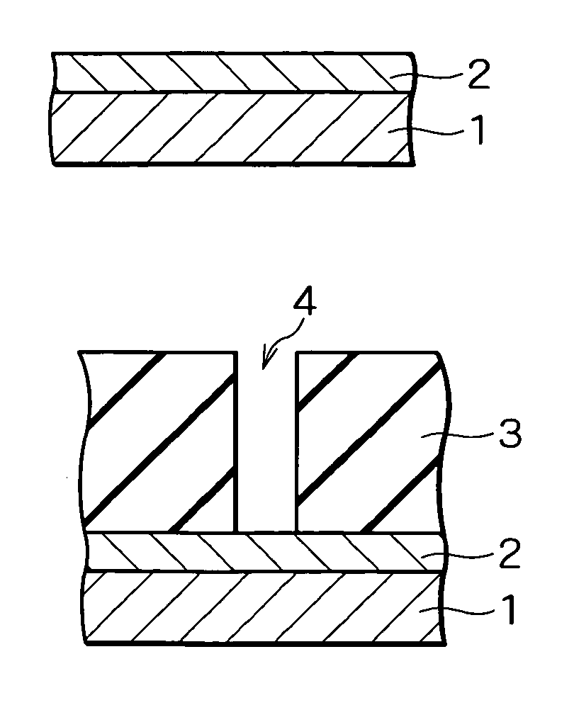
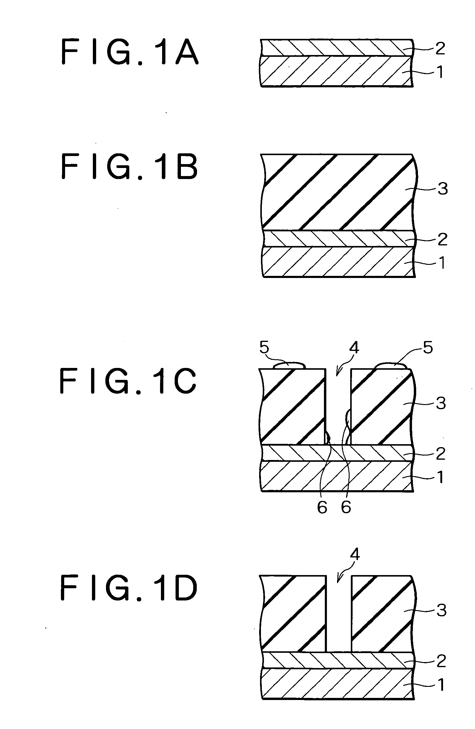
[0027] Preferred embodiments of the invention will be described below specifically with reference to the accompanying drawings. The present inventors conducted experiments and studies to overcome the problems, and discovered that the nickel silicide layer doped with an impurity, when exposed to plasma at the time of dry etching and ashing, turned the crystal state to amorphous and would become easily dissolvable in cleaning solution. The present inventors also found out that dissolution of the nickel silicide layer was influenced by the dissociation ions (HF2−) of the fluorine-containing compound.
[0028] To begin with, cleaning solution according to the first embodiment of the invention will be discussed. The cleaning solution according to the embodiment is a solution used in cleaning solution a substrate on which the nickel silicide layer is formed, and contains the fluorine-containing compound by 1.0 to 5.0 mass %, the chelating agent by 0.2 to 5.0 mass %, and the organic acid sal...
PUM
| Property | Measurement | Unit |
|---|---|---|
| Temperature | aaaaa | aaaaa |
| Percent by mass | aaaaa | aaaaa |
| Percent by mass | aaaaa | aaaaa |
Abstract
Description
Claims
Application Information