Memory device, display control driver with the same, and display apparatus using display control driver

Active Publication Date: 2005-01-06
RENESAS ELECTRONICS CORP
View PDF7 Cites 68 Cited by
  • Summary
  • Abstract
  • Description
  • Claims
  • Application Information

AI Technical Summary

Benefits of technology

[0015] Therefore, an object of the present invention is to provide a memory device for a display data, a display control driver with the memory d

Problems solved by technology

However, such a RAM is large in area and high in cost.
However, the one port RAM can not carry out the CPU write/read operation and the LCD read operation at a same time.
However, this conventional example contains the following problems.
During the wait time, however, the CPU 2 can not carry out other processes and is in the wait state.
As a result, the CPU 2 can not operate at an original operation speed.
In this way, the op

Method used


Image

  • Memory device, display control driver with the same, and display apparatus using display control driver
  • Memory device, display control driver with the same, and display apparatus using display control driver
  • Memory device, display control driver with the same, and display apparatus using display control driver

Examples


first embodiment

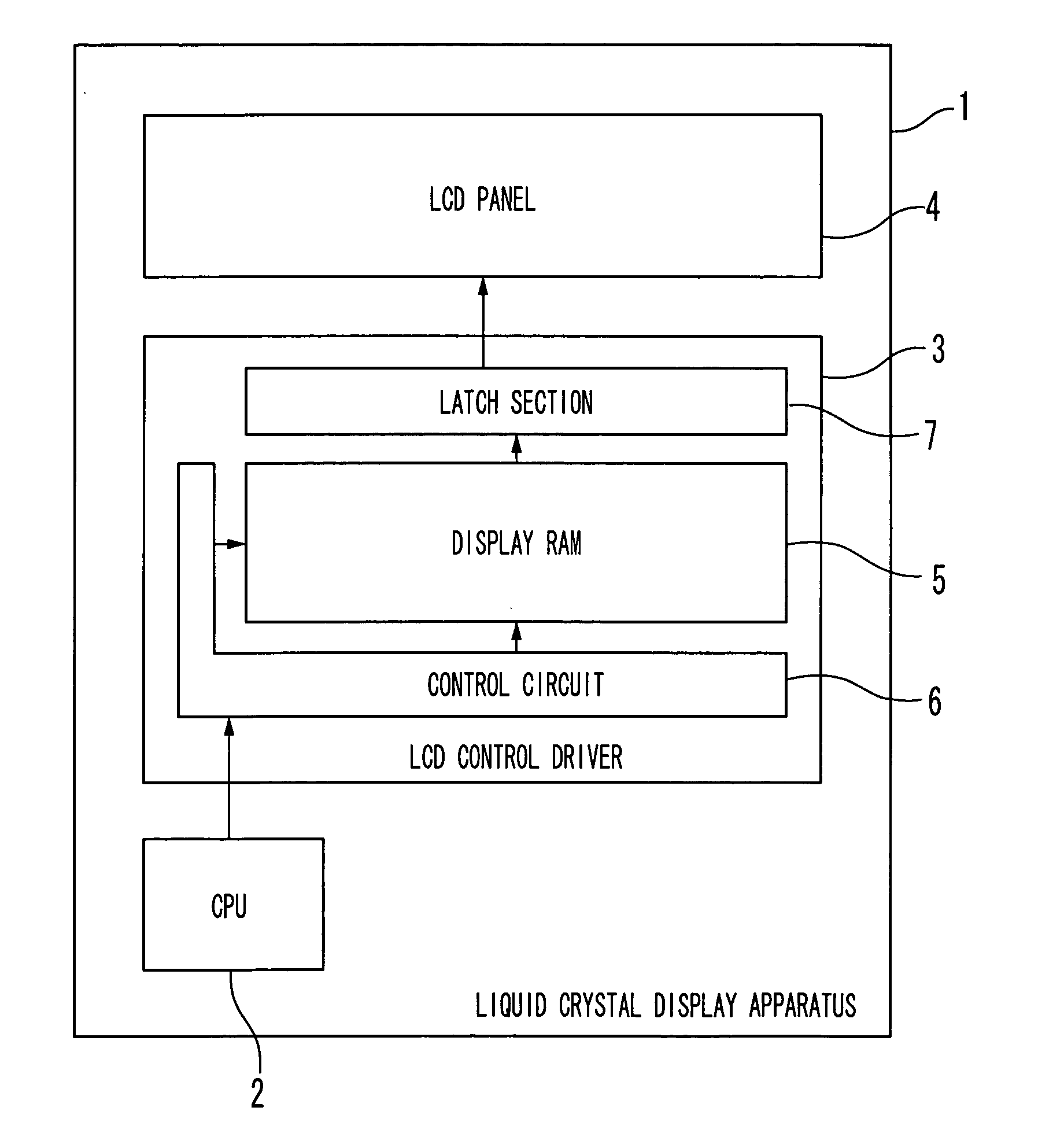
[0054] First, the LCD control driver according to the first embodiment of the present invention will be described. FIG. 5 is a block diagram showing an LCD apparatus including the LCD control driver with a memory device of a display data, according to the first embodiment. FIG. 6 is a circuit diagram showing the LCD control driver according to the first embodiment. FIGS. 7A to 7E are timing charts showing the operation of the LCD control driver. FIGS. 8A-1 to 8A-6 are diagrams showing the operation of the LCD control driver to cells, and FIGS. 8B-1 and 8B-2 are timing charts showing the operation of the LCD control driver.

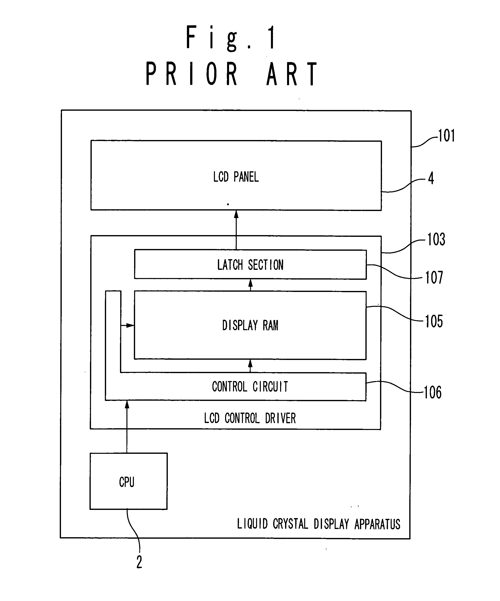
[0055] As shown in FIG. 5, the liquid crystal display (LCD) apparatus 1 includes a CPU 2, an LCD control driver 3 and an LCD panel 4. The LCD control driver 3 includes a display RAM 5 for storing a display data, a control circuit 6 for controlling the display RAM 5, and a latch section 7 for latching the display data for one horizontal line outputted from the disp...

second embodiment

[0074] The LCD control driver according to the second embodiment of the present invention will be described below. FIG. 9 is a circuit diagram showing the LCD control driver in the second embodiment, and FIG. 10 is a diagram showing a method of allocating an address of each of cells in the LCD control driver. In the first embodiment, the X addresses of the cells are allocated to increase one by one along the X-direction, as X=0, 1, 2, . . . , and the Y address is allocated to increase one by one along the Y-direction as Y=0, 1, 2, . . . Thus, the memory elements 8 of the display RAM is grouped into the plurality of banks along the X-direction. For this reason, as described in the first embodiment, the display data is horizontally written to the display RAM, namely, the CPU write operation is sequentially carried out on the cells arranged in the X-direction. In other wards, after the CPU write operation is carried out on one bank, the CPU write operation can be carried out on another...

third embodiment

[0083] The LCD control driver according to the third embodiment of the present invention will be described below. FIG. 11 is a circuit diagram showing the LCD control driver according to the third embodiment. FIG. 12 is a diagram showing a method of allocating X addresses of the cells in the LCD control driver. FIGS. 13A-1 to 13A-8 are diagrams showing the operation of the LCD control driver for each cell, and FIGS. 13B-1 and 13B-2 are timing charts showing the operation of the LCD control driver.

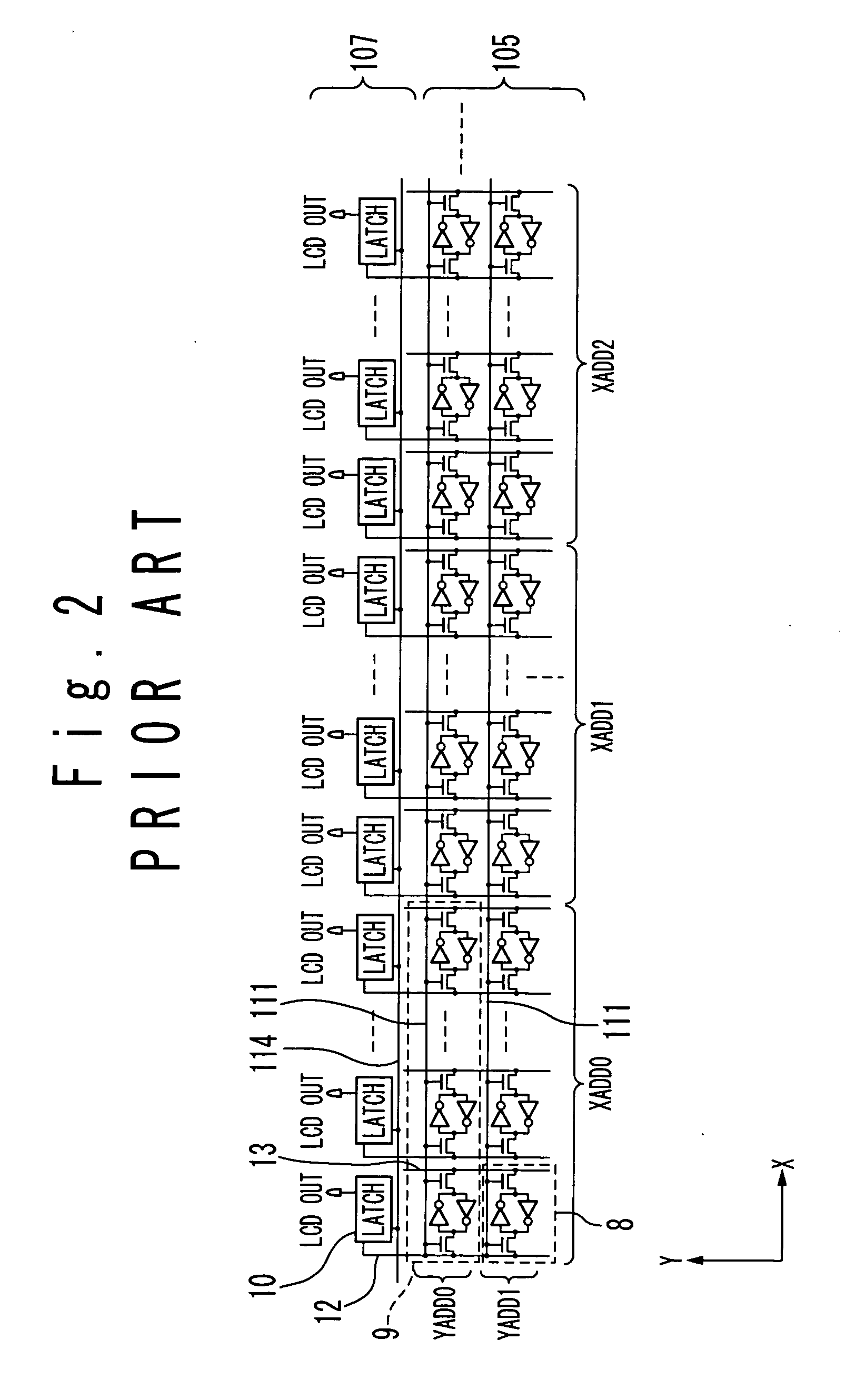
[0084] In the first embodiment, the memory elements 8 of the display RAM are grouped into the banks for every column, and each bank contains one column of cells. However, in the third embodiment, as shown in FIGS. 11 and 12, the memory elements 8 of the display RAM are grouped into the banks such that the two columns of cells are contained in one bank. From the left end of FIGS. 11 and 12, the banks are arranged as a bank A, a bank B, a bank C, . . . . One LCD word line 11a, one CPU word l...


PUM


Abstract

A memory device includes a memory and a control circuit. The memory includes cells arranged in a matrix of rows and columns. The cells are grouped into banks, and each of the banks contains at least one column of the cells. The control circuit instructs a read operation in units of rows and a write operation in units of cells, and inhibits the read operation in units of the banks when the write operation is carried out to a specific one of the cells of a specific one of the banks.

Description

BACKGROUND OF THE INVENTION [0001] 1. Field of the Invention [0002] The present invention relates to a memory device, a display control driver with the same, and a display apparatus using the display control driver. [0003] 2. Description of the Related Art [0004]FIG. 1 is a block diagram showing a conventional liquid crystal display apparatus (LCD). As shown in FIG. 1, an LCD 101 includes a CPU 2 for generating a display data, an LCD control driver 103, and an LCD panel 4 for displaying the display data. The LCD control driver 103 stores the display data generated by the CPU 2 for a one screen and then outputs the held display data for one horizontal line to the LCD panel 4 at a time. The LCD control driver 103 is composed of a display RAM (Random Access Memory) 105 for storing the display data, a control circuit 106 for controlling the display RAM 105, and a latch section 107 for latching the display data for one horizontal line outputted from the display RAM 105, and then outputti...

Claims


Application Information

Patent Timeline
IPC IPC(8): G09G3/36G09G5/39G09G5/00
CPCG09G3/3611G09G3/3685G09G3/3688G09G5/001G09G2360/18G09G2310/027G09G2310/08G09G2320/0252G09G2330/021G09G2310/0248G09G3/36
Inventor SHIONO, MASUMI
Owner RENESAS ELECTRONICS CORP
Why Eureka
Try Eureka