
Memory system having data inversion and data inversion method for a memory system

a memory system and data inversion technology, applied in the field of memory systems, can solve the problems of increasing the pin overhead of the memory device, unable to selectively apply data inversion to individual bytes during a data write operation, and unable to achieve data write operation selectively

Active Publication Date: 2005-01-06
SAMSUNG ELECTRONICS CO LTD
View PDF4 Cites 17 Cited by
  • Summary
  • Abstract
  • Description
  • Claims
  • Application Information

AI Technical Summary

Benefits of technology

[0005] Generally, it is a goal to improve the data transfer speed of a memory system. To this end, various techniques are employed to improve the high frequency characteristics (speed) of a memory device. For some memory devices, a data inversion scheme is employed to reduce the simultaneous switching noise in the device and thereby improve the high frequency operating characteristics. An example of such a memory device and associated memory system will now be described in further detail.
[0012] The data inversion block 115 reduces the simultaneous switching noise in the input / output buffers of the memory device 100 and thereby improves the high frequency characteristics of the device.
[0018] For one thing, an additional pin (DIM pin) is required for the write data inversion flag. This increases the pin overhead of the memory device.
[0019] For another thing, only one write data inversion flag is provided for all of the data inputs (e.g., 32 DQ input pins) of the memory device. So, with the device and method illustrated in FIGS. 1-8, it is not possible to selectively apply data inversion to individual bytes during a data write operation. Meanwhile, applying write data inversion on a byte-by-byte basis improves the high frequency operation of the device.

Problems solved by technology

However, there are drawbacks to memory system with data inversion as described above.
This increases the pin overhead of the memory device.
So, with the device and method illustrated in FIGS. 1-8, it is not possible to selectively apply data inversion to individual bytes during a data write operation.

Method used


Image

  • Memory system having data inversion and data inversion method for a memory system
  • Memory system having data inversion and data inversion method for a memory system
  • Memory system having data inversion and data inversion method for a memory system

Examples


Embodiment Construction

[0039]FIG. 9 shows one embodiment of a memory system 2 operating with data inversion. The memory system 2 includes a memory device 500 and a memory controller 600. In clear distinction from the memory system 1 of FIG. 1, the memory system 2 does not include any DIM signal between the memory controller 400 and the memory device 300.

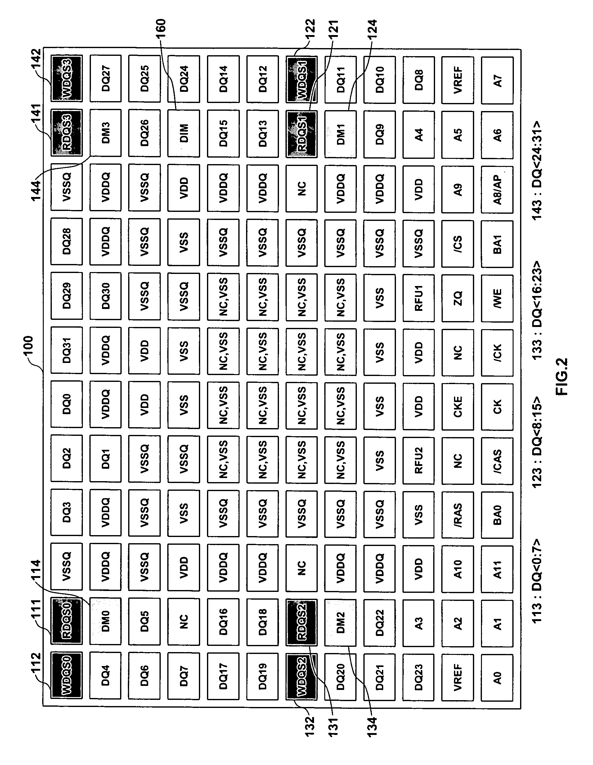
[0040]FIG. 10 shows an exemplary ball (or pin) configuration of the memory device 300. As can be seen from FIG. 10, the balls (or pins) of the memory device 500 similar to those for the memory device 100 shown in FIG. 2, except that the memory device 500 does not include the DIM pin 160, and instead has an extra unused (NC) pin 360. Also, the balls / pins 311, 321, 331 and 341 in FIG. 10 are named RDQS,WFLAG, and the balls / pins 312, 322, 332 and 342 in FIG. 10 are named WDQS,RFLAG, as will be explained in greater detail below.

[0041]FIG. 11 shows a data processing block diagram of one embodiment of the memory device 300. The memory device 300 includes data ...


PUM


Abstract

A memory system and a method of reading and writing data to a memory device provide byte-by-byte write data insertion without adding extra pins or balls to the packaged device. Accordingly, the high frequency performance of the device can be improved.

Description

CROSS-REFERENCES TO RELATED APPLICATIONS [0001] This application claims priority under 35 U.S.C § 119 from Korean Patent Application No. 2003-44846, filed on 3 Jul. 2003 the entirety of which is hereby incorporated by reference for all purposes as if fully set forth herein.BACKGROUND AND SUMMARY [0002] 1. Field [0003] This invention pertains to the field of memory systems, and more particularly, to a memory system having data inversion, and to a method of data inversion for a memory system. [0004] 2. Description [0005] Generally, it is a goal to improve the data transfer speed of a memory system. To this end, various techniques are employed to improve the high frequency characteristics (speed) of a memory device. For some memory devices, a data inversion scheme is employed to reduce the simultaneous switching noise in the device and thereby improve the high frequency operating characteristics. An example of such a memory device and associated memory system will now be described in f...

Claims


Application Information

Patent Timeline
Patent Type & Authority Applications(United States)
IPC IPC(8): G06F13/16G06F12/00G06F12/04G11C7/00G11C7/10G11C11/401
CPCG11C7/1006G11C7/1051G11C7/1096G11C7/1078G11C7/109G11C7/1063G11C7/00
Inventor JANG, SEONG-JIN
Owner SAMSUNG ELECTRONICS CO LTD
Features
  • Generate Ideas
  • Intellectual Property
  • Life Sciences
  • Materials
  • Tech Scout
  • Unparalleled Data Quality
  • Higher Quality Content
  • 60% Fewer Hallucinations
Learn More