Plasma display device and driving method used for same

a technology of plasma display device and display panel, which is applied in the direction of gas discharge vessel/container, address electrode, instrument, etc., can solve the problems of deteriorating less stable occurrence of writing discharge, and conventional plasma display device described above, so as to improve the contrast ratio, improve the quality of the display screen, and reduce the luminance of ligh

Inactive Publication Date: 2005-01-13
PIONEER CORP
View PDF9 Cites 19 Cited by
  • Summary
  • Abstract
  • Description
  • Claims
  • Application Information

AI Technical Summary

Benefits of technology

In view of the above, it is a first object of the present invention to provide a plasma display device capable of obtaining a high-quality display screen by lowering light-emitting luminance in black display to improve a contrast ratio. I

Problems solved by technology

However, when a plasma display device is used in a dark environment or when dark images are to be displayed, luminance in black display becomes a factor which degrades quality of a display screen.
However, the conventional plasma display device described above has a following problem.
Hei08-222036, in order to lower black display luminance, pre-discharge operations are thinned out However, this method has a problem, that is, during a sub-field during which no pre-discharge is made to occur or in a unit cell in which no pre-discharge is made to occur, occurrence of writing discharge is less stable compared with that of writing discharge during a sub-field during which the pre-discharge was made to occur or in a unit cell in which the pre-discharge was made to occur and, therefore, proper image display cannot be realized.
Particularly, in a unit cell in which pre-discharge operations are thinned out continuously in two or more sub-fields, occurrence of writing discharge becomes remarkably unstable, thus causing a flicker in displayed images, occurrence of cells being not lit, or a like.
However, this method has a problem, that is, since a difference between a lowering ratio of maximum luminance and a lowering ratio of black luminance is small, an effect of improving a contrast ratio is small.
Next, problems with a second conventional technology are described.
The reason for this is that, in an AC (Alternating Current)-type plasma display device, modulation of light-emitting display luminance by a voltage is difficult and changing of a number of light-emitting times is required for the modulation of the luminance.
However, in the PDP having such the configurations as sho

Method used


Image

  • Plasma display device and driving method used for same
  • Plasma display device and driving method used for same
  • Plasma display device and driving method used for same

Examples


first embodiment

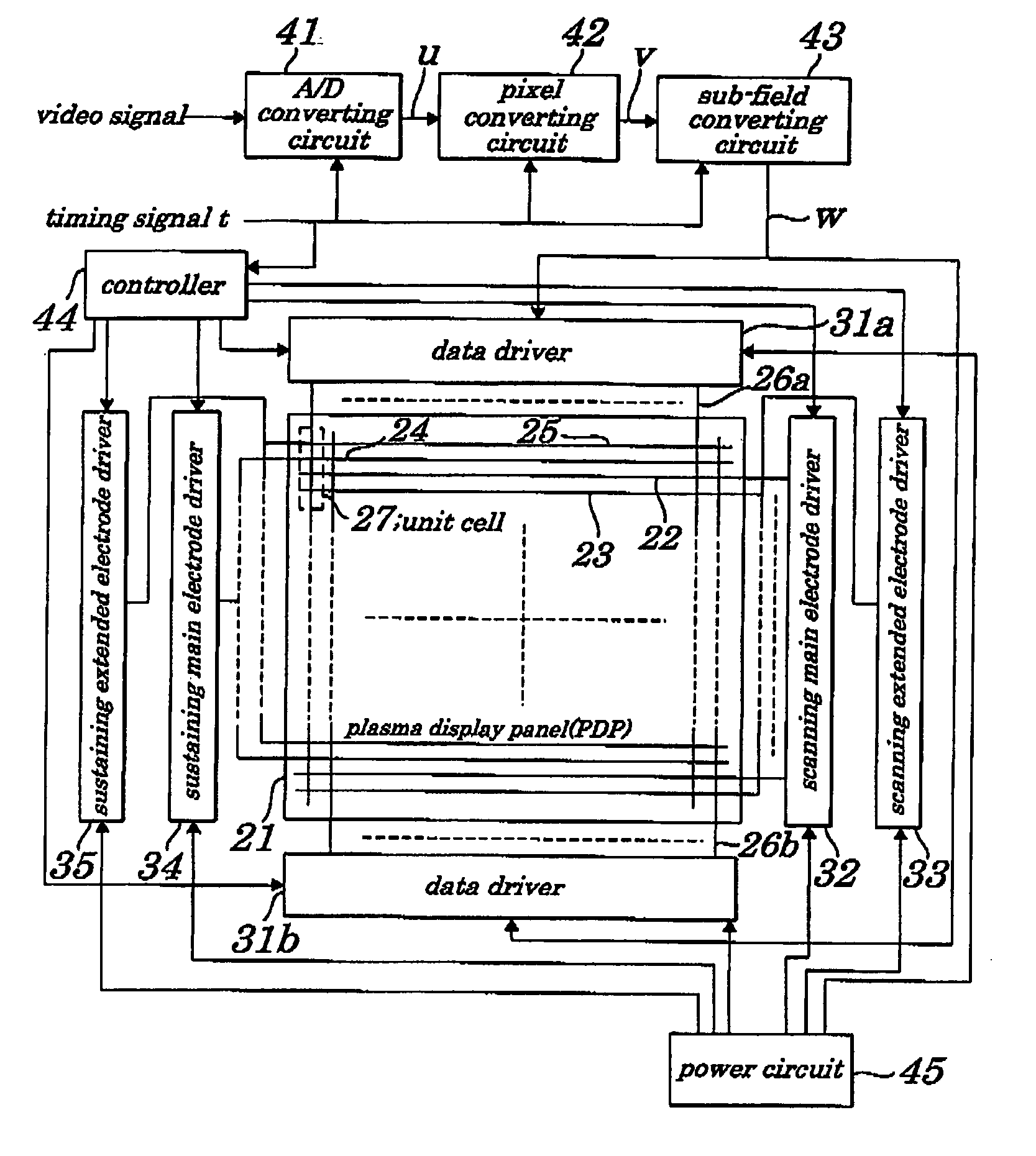
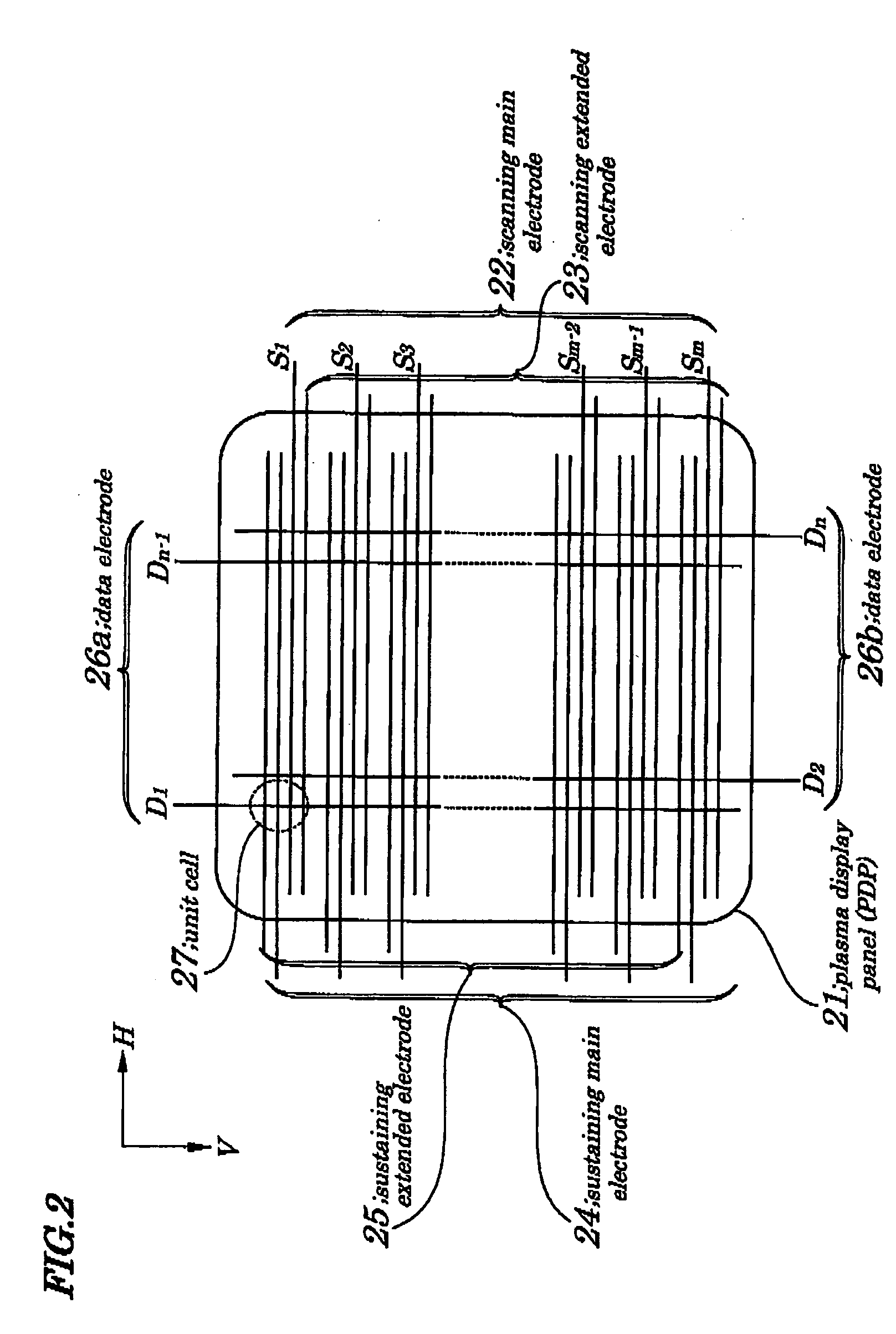
FIG. 1 is a schematic block diagram showing electrical configurations of a plasma display device according to a first embodiment of the present invention. The plasma display device of the first embodiment, as shown in FIG. 1, includes a plasma display panel (PDP) 21, data drivers 31a and 31b, a scanning main electrode driver 32, a scanning extended electrode driver 33, a sustaining main electrode driver 34, a sustaining extended electrode driver 35, an A / D (Analog / Digital) converting circuit 41, a pixel converting circuit 42, a sub-field converting circuit 43, a controller 44, and a power circuit 45.

In the PDP 21, a front substrate (not shown) and a rear substrate (not shown) are arranged in a manner in which the front substrate faces the rear substrate. On a surface of the front substrate facing the rear substrate, a scanning main electrode 22 and a sustaining main electrode 24 are arranged in parallel to each other with a discharge gap (not shown) being interposed between the sc...

second embodiment

FIG. 7 is a plan view illustrating configurations of a unit cell 27 of a PDP according to a second embodiment of the present invention in which same reference numbers are assigned to components having the same function as in the first embodiment shown in FIG. 3. FIG. 8 is a cross-sectional view of the unit cell 27 taken along a line A-A of FIG. 7.

In the unit cell 27 of the PDP of the second embodiment, a black dielectric layer 58 is formed on a scanning main electrode 22 and a sustaining main electrode 24. The black dielectric layer 58 is formed in a manner in which it covers directly a region including the scanning main electrode 22, sustaining main electrode 24, bus electrodes 22a and 24a, and a discharge gap 29 as shown in FIG. 3. As shown in FIG. 8, the black dielectric layer 58 is formed in a transparent dielectric layer 53. In this case, the transparent dielectric 53 is formed so as to cover all the electrodes on which the black dielectric layer 58 is stacked and further the...

third embodiment

FIG. 9 is a plan view illustrating configurations of a unit cell 27 of a PDP according to a third embodiment of the present invention in which same reference numbers are assigned to components having the same function as in the first embodiment shown in FIG. 7. FIG. 10 is a cross-sectional view of the unit cell taken along a line A-A of FIG. 9. In the unit cell of the PDP of the third embodiment shown in FIG. 9, instead of the black dielectric layer 58 shown in FIG. 7, a black dielectric layer 58A is mounted, which is formed in a region being different from the region in which the black dielectric layer 58 is formed. The black dielectric layer 58A, as shown in FIG. 10, is formed almost only above the discharge gap 29 and not above the scanning main electrode 22 and the sustaining main electrode 24.

In the PDP of the third embodiment, light emitted in a portion of the discharge gap 29 is shielded by the black dielectric layer 58A and light emitted on the scanning main electrode 22 a...


PUM


Abstract

A plasma display device is provided which is capable of solving a problem that luminance of a black display caused by light emitted by pre-discharge and pre-erasing discharge is high, of enhancing a contrast ratio by lowering display luminance, of reducing discharge currents that flow by writing discharge without lowering display luminance. By dividing surface discharge electrodes on a side where writing discharge is made to occur into first and second portions, writing discharge to select a state of being displayed or being non-displayed is made to occur by using only the first portion. Then, sustaining discharge to realize light-emission for displaying is made to occur by using the first and second portions. This causes currents that flow by writing discharge to decrease and writing operations to be performed in a stable manner. Since no reduction in currents that flow by sustaining discharge occurs, displaying at high luminance can be maintained.

Description

BACKGROUND OF THE INVENTION 1. Field of the Invention The present invention relates to a plasma display device and a method for driving the plasma display device and a plasma display panel making up the plasma display device and more particularly to the plasma display device that can be suitably used to improve a contrast ratio of a display screen and to the plasma display panel that can achieve stable luminance-enhanced display at low costs and to the driving method to be used in the plasma display device having the plasma display panel. 2. Description of the Related Art First, first conventional technology and its problems to be solved are described. A plasma display device including a plasma display panel (hereinafter may be referred simply to as a “PDP”) as its main component has many features in that it can be of a thin-type, it can display images on a large screen with comparatively easiness, and it can provide a wide viewing angle and a high speed response. Therefore, in ...

Claims


Application Information

Patent Timeline
IPC IPC(8): G09G3/20G09G3/288G09G3/291G09G3/292G09G3/293G09G3/294G09G3/298H01J11/22H01J11/24H01J11/26H01J11/34
CPCG09G3/2927G09G3/293G09G2330/025G09G3/2986G09G2320/0238G09G3/294H01J11/22H01J11/24
Inventor TANAKA, YOSHITOMAKINO, MITSUYOSHI
Owner PIONEER CORP
Why Eureka
Try Eureka