Semiconductor memory apparatus and self-repair method

a memory apparatus and semiconductor technology, applied in the direction of digital storage, electronic circuit testing, instruments, etc., can solve the problems of almost impossible to increase the yield to 100%, the apparatus cannot of course be shipped as a product, and the yield becomes a problem

Inactive Publication Date: 2005-01-13
SONY CORP
View PDF5 Cites 11 Cited by
  • Summary
  • Abstract
  • Description
  • Claims
  • Application Information

AI Technical Summary

Benefits of technology

[0015] It is thus an object of the present invention addressing the problems described above to provide a semiconductor memory apparatus capable of carrying out a repair search at a high speed but at a small circuit scale in a configuration providing a BIST circuit embedded in the semiconducto

Problems solved by technology

In a semiconductor memory apparatus such as a DRAM, the integration scale is extremely large and, in consequence, the yield becomes a problem.
Practically, it is almost impossible to increase the yield to 100% so that one may assume that a defective memory cell always exists in a semiconductor memory apparatus.
If a defective memory cell exists in a semiconductor memory apparatus, however, the apparatus cannot of course be shipped as a product.
It is thus practically difficult to test the individual memories of the same LSI chip independently of each other.
In addition, as the operating speed of the LSI chip becomes higher, it becomes difficult to evaluate the performance of a memory by using an external memory tester.
In addition, eve

Method used


Image

  • Semiconductor memory apparatus and self-repair method
  • Semiconductor memory apparatus and self-repair method
  • Semiconductor memory apparatus and self-repair method

Examples


first embodiment

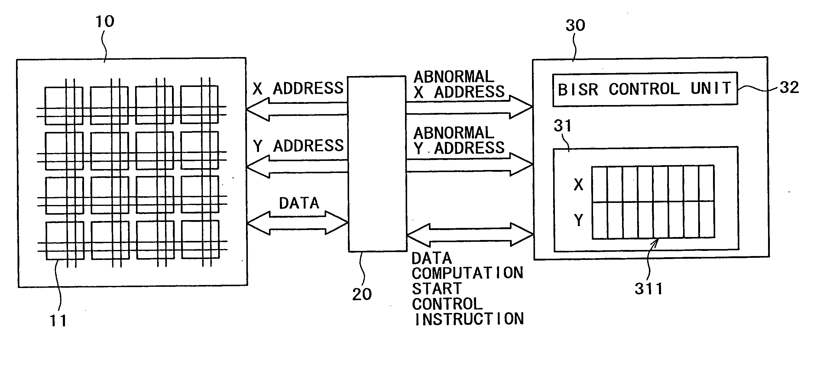
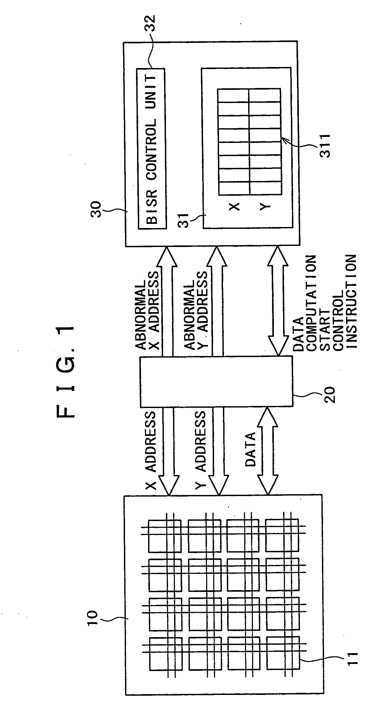
[0072]FIG. 6 is a block diagram showing a typical configuration of a BISR circuit 30A provided by a first embodiment. As shown in FIG. 6, the BISR circuit 30A implemented by the first embodiment includes buffer units 41-1 to 41-4 each including address-pair storage locations and flags, an X-mask-address storage unit 42 and Y-address confirmation units 43-1 to 43-4. An overflow bit is a BISR result indicating whether or not the address of an abnormal bit is repairable.

[0073] When the BIST circuit 20 finishes an evaluation process to determine whether each memory cell is normal or abnormal, the BIST circuit 20 supplies a BISRSTART start signal to start a BISR computation to the BISR circuit 30A. Receiving the BISRSTART start signal, the BISR circuit 30A starts the BISR computation. As the BISR computation is finished, the BISR circuit 30A outputs a BISREND end signal indicating that the BISR computation has been finished.

[0074] In the configuration shown in FIG. 6, each of the buffe...

second embodiment

[0092]FIG. 7 is a block diagram showing a typical configuration of a BISR circuit 30B implemented by a second embodiment. Components employed in the second embodiment as components identical with their counterparts included in the first embodiment shown in FIG. 6 are denoted by the same reference numerals as the counterparts. As is obvious from FIG. 7, the BISR circuit 30B includes buffer units 41-1 to 41-4 and Y-address confirmation units 43-1 to 43-4. Each of the buffer units 41-1 to 41-4 has address-pair storage locations each used for storing a pair of addresses and has flags associated with the address-pair storage locations. In each of the buffer units 41-1 to 41-4, flags associated with a particular address-pair storage location are linked to flags associated with address-pair storage locations adjacent to the particular address-pair storage location in a chain connection to form shift registers. As many such shift registers as row redundant lines 14 connected in the in the Y...

third embodiment

[0104] In the case of the first and second embodiments, as the Y-address storage unit 431 employed in each of the Y-address confirmation units 43-1 to 43-4 as a unit for confirming Y addresses, 2 Y-address storage locations are provided. In the case of a third embodiment, Y shift registers 413 are employed as shown in FIG. 8 in place of the Y-address storage unit 431. The Y shift registers 413 are used for implementing a method to confirm Y addresses in accordance with the third embodiment.

[0105] To put it concretely, as many Y shift registers 413 as column redundant lines 15 connected in the X directions are employed. In the case of the third embodiment, the number of Y shift registers 413 is 2. Pointers of the Y shift registers 413 are each shifted at one time. If a Y address stored at a Y-address storage location pointed to by a combination of pointer positions is the same as the Y address stored at an address pair in the buffer units 41-1 to 41-4, the address pair is masked. A ...


PUM


Abstract

In a memory unit provided by the present invention, unit blocks are laid out to form a block matrix. Each of the unit blocks has a plurality of memory cells arranged to form a cell matrix and a redundant line including a redundant memory cell. A plurality of unit blocks in the block matrix forms a one-dimensional group oriented in a first or second direction so that unit blocks pertaining to each one-dimensional group share a redundant line. Self-repair means embedded in the same chip as the memory unit stores only a minimum number of address pairs required for determining a redundant line to be used for repairing an abnormal memory cell for each unit block in storage means. The address of the redundant line to be used for repairing an abnormal memory is then found for each unit block on the basis of the minimum number of address pairs stored in the storage means. By storing only minimum required address information as such, a small size of the storage means and, hence, small circuit scales are sufficient. In addition, since a repair search is carried out by the embedded self-repair means in the same chip as the memory unit, the repair search can be carried out at a high processing speed.

Description

BACKGROUND OF THE INVENTION [0001] The present invention relates to a semiconductor memory apparatus such as a DRAM (Dynamic Random Access Memory) or an SRAM (Static Random Access Memory) as well as relates to a self-repair method adopted in the semiconductor memory apparatus. More particularly, the present invention relates to a semiconductor memory apparatus having a redundancy search circuit for replacing a bad (defective) memory cell with a redundant memory cell included in the semiconductor memory apparatus in advance as well as relates to a self-repair method adopted in the semiconductor memory apparatus. [0002] In a semiconductor memory apparatus such as a DRAM, the integration scale is extremely large and, in consequence, the yield becomes a problem. Practically, it is almost impossible to increase the yield to 100% so that one may assume that a defective memory cell always exists in a semiconductor memory apparatus. A defective memory cell is also referred to hereafter as a...

Claims


Application Information

Patent Timeline
IPC IPC(8): G11C29/00G01R31/28G11C29/04G11C29/12G11C29/44
CPCG11C11/401G11C29/44G11C2207/104G11C29/72G11C2029/1208G11C29/4401
Inventor NAGATA, KOUKODAMA, HIROAKI
Owner SONY CORP
Why Eureka
Try Eureka