Electron emitter with epitaxial layers

a technology of electron emitters and epitaxial layers, applied in the field of microelectronics, can solve the problems of high vacuum operation requirements problems and unresolved needs of flat emitters, and general difficulty and cost of manufacture of spindt tip emitters

Inactive Publication Date: 2005-01-27
HEWLETT PACKARD DEV CO LP
View PDF9 Cites 9 Cited by
  • Summary
  • Abstract
  • Description
  • Claims
  • Application Information

AI Technical Summary

Problems solved by technology

Manufacturing of Spindt tip emitters is generally difficult and costly.
Also, Spindt tip emitters require high vacuum for operation.
Problems and unresolved needs remain with flat emitters, however.
For example, emitted electron beams can suffer significant divergence.
This can be disadvantageous in emitter applications in which the emitted electrons are to be directed to a defined target area.
One significant source of electron beam divergence is electric field non-uniformities arising from non-planarity in the emitter surface and other electric defects to dielectric, conductor, and electron source layers.
Also, thickness irregularities and other layer inconsistencies may lead to layer regions that have a reduced resistance compared to other regions.
These regions may experience a higher current flux than other layer regions, which may in turn increase the temperature of the region that further lowers resistance.
The cycle of continually increasing temperature and continually reduced resistance may ultimately result in breakdown of the region.
Thicker layers, however, increase the required turn-on voltage of the emitter, lower emitter efficiency, and increase emission scatter.

Method used


Image

  • Electron emitter with epitaxial layers
  • Electron emitter with epitaxial layers
  • Electron emitter with epitaxial layers

Examples


Embodiment Construction

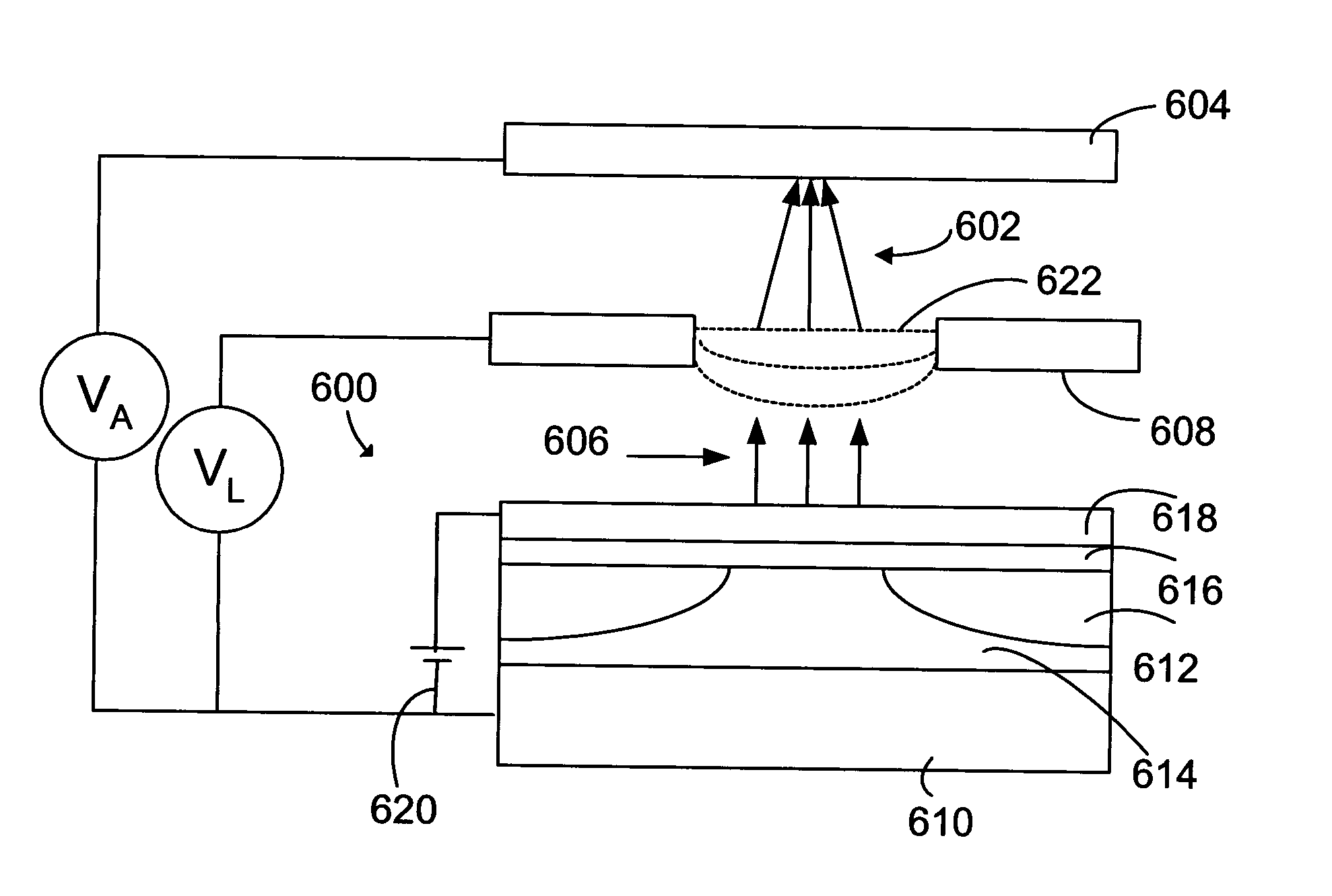
[0017] The present invention is directed to emitter devices, methods for emitting electrons, and methods for making emitters. An exemplary emitter of the invention includes a single crystal electron source, a thin conductor layer, and an epitaxial dielectric layer between the conductor and the source layer. When an electric field is generated between the conductor layer and the electron source across the dielectric layer, electrons are emitted from the source. The electrons transport through the dielectric via tunneling or the like and are emitted from the surface of the conductor layer. The epitaxial dielectric layer and the conductor layers are substantially flat and free from geometrical and electrical defects. The electric field across the dielectric is therefore substantially uniform and unidirectional. As a result, electrons can be emitted substantially free of electrical field induced divergence.

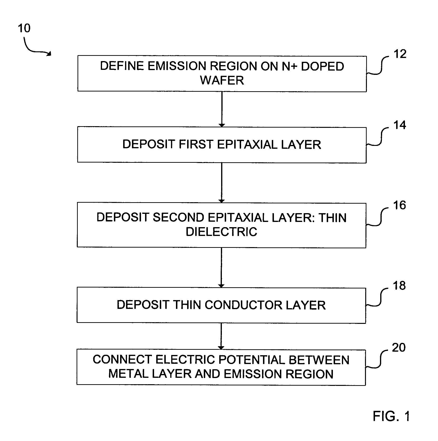
[0018]FIG. 1 is a flowchart illustrating a first method 10 for making an emitter...


PUM


Abstract

An emitter includes a single crystal electron source, an epitaxial layer, and a thin conductor layer. When an electric field is induced from the conductor across the epitaxial layer, electrons are emitted from the electron source, transported through the epitaxial layer, and are emitted from the conductor layer.

Description

FIELD OF THE INVENTION [0001] The invention is in the microelectronics field. The invention particularly concerns emitters and devices incorporating emitters. BACKGROUND OF THE INVENTION [0002] Emitters have a wide range of potential applicability in the microelectronics field. An emitter emits electrons in response to an electrical signal. The controlled emissions form a basis to create a range of useful electrical and optical effects. Prior conventional emitters include Spindt tip cold cathode devices as well as flat emitters. Challenges presented by Spindt tip emitters include their manufacturability and stability over their service life. Manufacturing of Spindt tip emitters is generally difficult and costly. Also, Spindt tip emitters require high vacuum for operation. [0003] Traditional flat emitters are comparably advantageous because they present a larger emission surface that can be operated in less stringent vacuum environments. Flat emitters include a dielectric emission la...

Claims


Application Information

Patent Timeline
Patent Type & Authority Applications(United States)
IPC IPC(8): H01J1/312H01J9/02
CPCB82Y10/00H01J9/027H01J1/312
Inventor NOVET, THOMASBENNING, PAUL J.GOVYADINOV, ALEXANDERBICKNELL-TASSIUS, ROBERT
Owner HEWLETT PACKARD DEV CO LP
Why Eureka
Try Eureka