Power transfer measurement circuit for wireless systems

a power transfer and wireless system technology, applied in the direction of antennas, transmission, modulation, etc., can solve the problems of unnecessary energy consumption of pa, unsatisfactory output signal emission, and low efficiency

Active Publication Date: 2005-01-27
SIGE SEMICON
View PDF8 Cites 18 Cited by
  • Summary
  • Abstract
  • Description
  • Claims
  • Application Information

AI Technical Summary

Problems solved by technology

Any portion of the signal provided to the load that is not transferred reflects back into an output port of the PA and results in the PA producing unwanted signal emissions and lower efficiency.
If a wireless device does not fall within these standards, then such a wireless device is not salable, since broadcasting of RF signals outside a designated frequency band for the wireless devices is known to cause interference to surrounding electrical devices.
Furthermore, if the amplified RF output signal reflects back from the load, then less than a maximum transfer of RF signal power occurs and this results in unnecessary energy consumption by the PA.
In addition to reduced power efficiency, amplified signals reflected back into the PA can damage the PA as relatively high voltages build on the output terminals of the circuit.
Rather, this energy can be absorbed by the PA circuit resulting in a rise in junction temperatures concomitant with the loss of net power amplifier efficiency.
This standing wave results in wasted energy and thus leads to wireless system inefficiencies.
Typically, a peak voltage detection scheme is utilized and it is therefore directly affected by a VSWR mismatch error.
Unfortunately, with this technique, no indication of a level of VSWR mismatch is provided because the rise in peak voltage can be attributed to an increase in output power from the PA or a change in the VSWR.
Unfortunately, this technique implements a peak voltage detection scheme and is therefore directly affected by VSWR mismatch error.
A disadvantage however, is that the final amplification stage is typically outside a control loop of the PA.
Thus, the RF output signal is typically susceptible to supply voltage and temperature changes in the final amplification stage of the PA.
Unfortunately, this approach has a number of off-chip components and often the detectors used for such an approach do not have the temperature stability of on-chip detectors.

Method used


Image

  • Power transfer measurement circuit for wireless systems
  • Power transfer measurement circuit for wireless systems
  • Power transfer measurement circuit for wireless systems

Examples


first embodiment

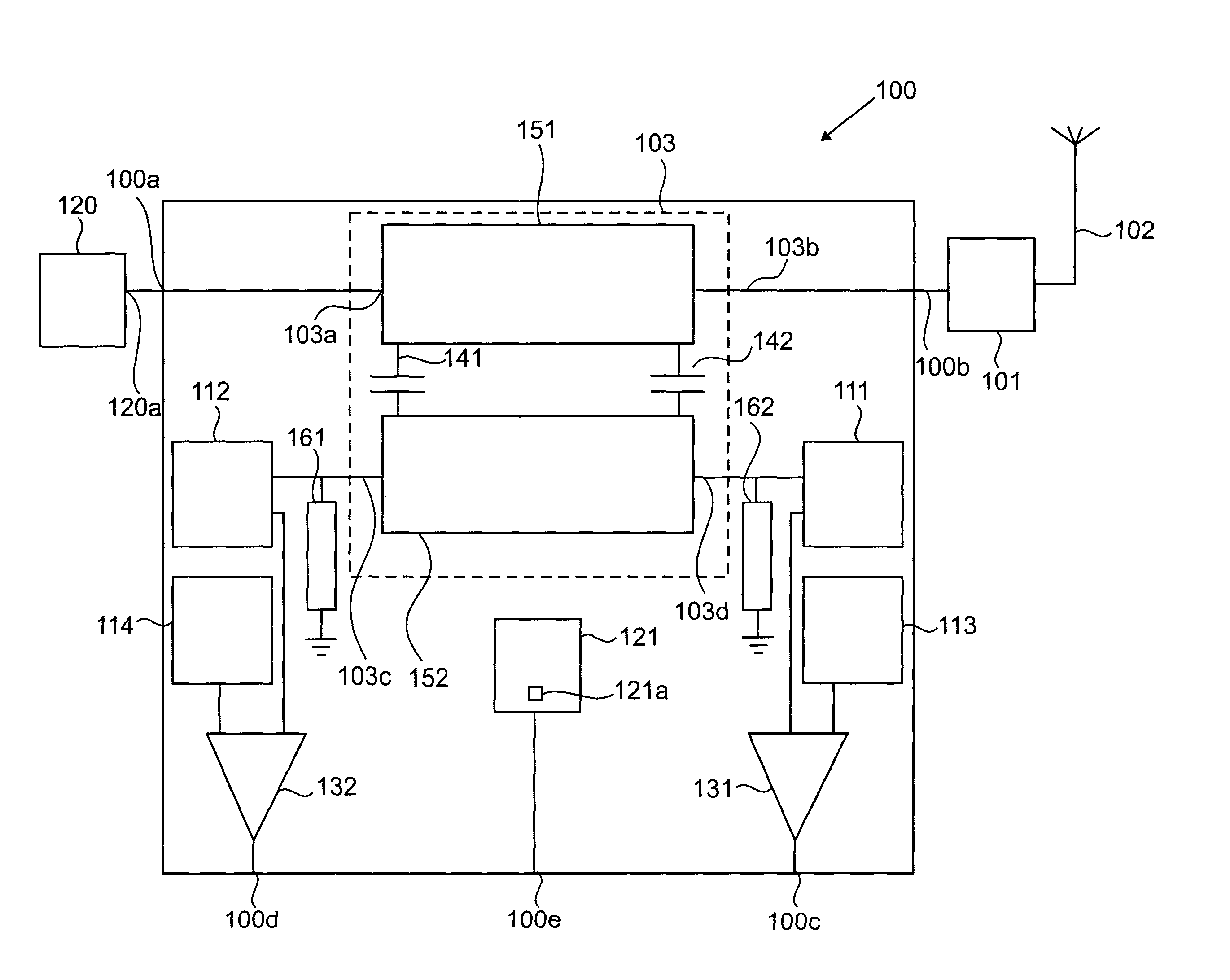
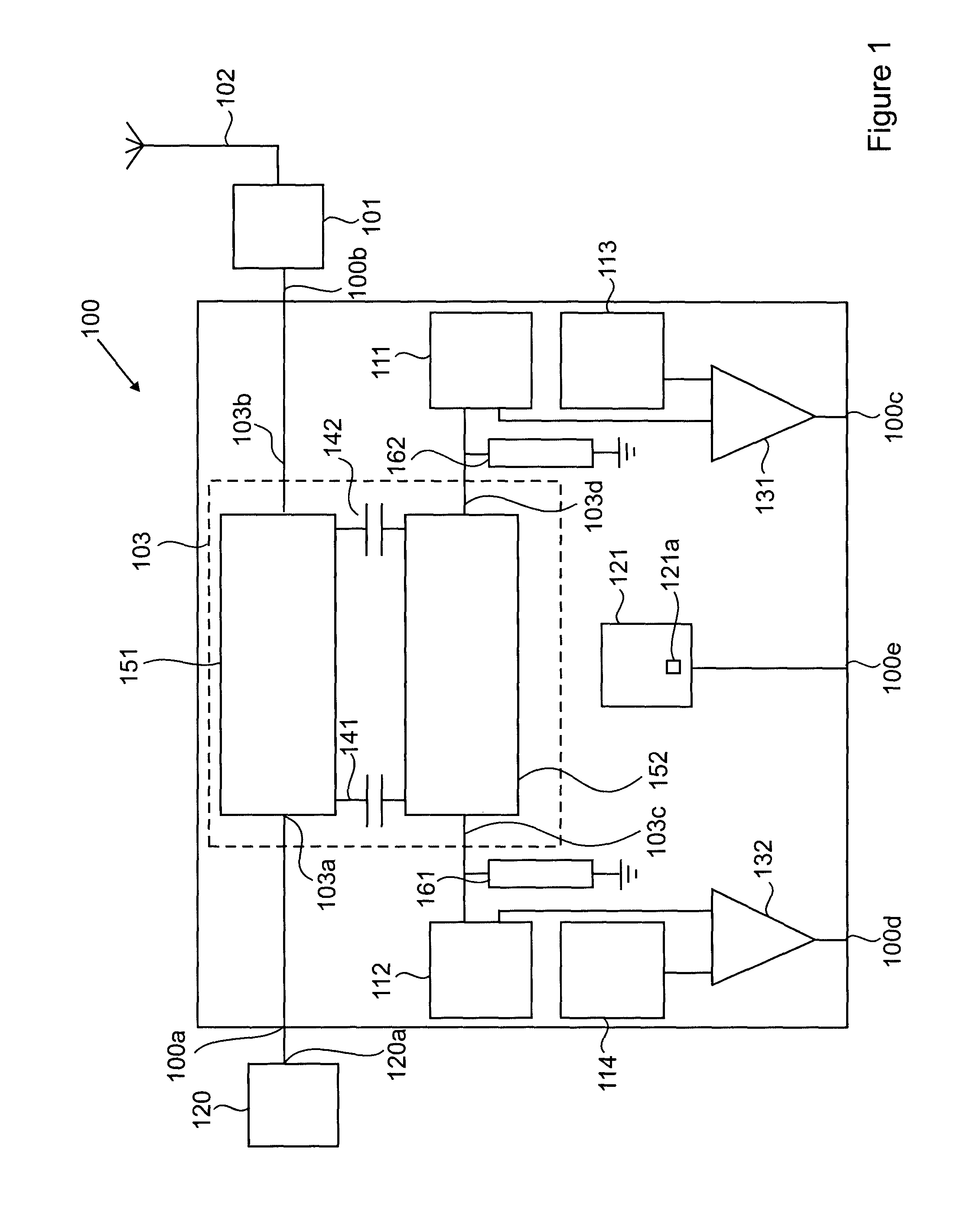
[0015]FIG. 1 illustrates a coupler and detector circuit (CDC) 100 having an internal signal path, in accordance with the invention. A power amplifier (PA) circuit 120 is disposed for providing an amplified RF output signal via an output port thereof 120a to a first node 100a of the CDC 100. Within the CDC the amplified RF output signal propagates through a RF coupler, in the form of a quarter wave coupler circuit 103, from a first port thereof 103a to a second port thereof 103b, along a main signal path 151, disposed between a first node 100a directly connected to the PA output port 120a, and a second node 100b directly connected, at an input of the feedline circuit 101. The feedline circuit 101 is disposed between a RF antenna 102 and the second node 100b of the CDC 100, where the antenna 102 is used to broadcast the amplified RF output signal. The second port 103b of the quarter wave coupler is directly connected to the second node 100b of the CDC 100. The energy of the amplified ...

second embodiment

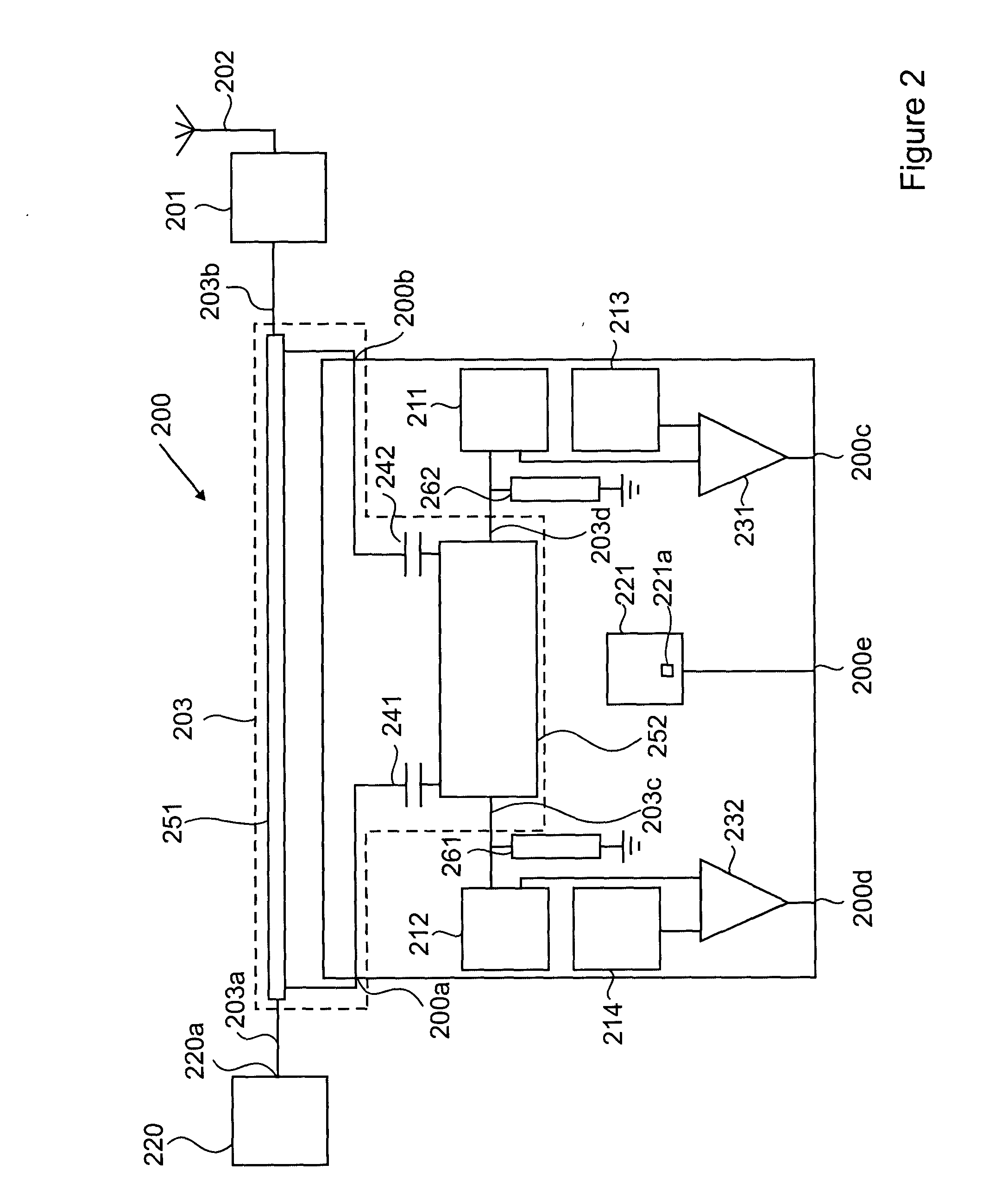
[0022]FIG. 2 illustrates a coupler and detector circuit (CDC) 200 having an external signal path, in accordance with the invention. The external signal path, in the form of a main signal path 251, is not disposed on a same semiconductor die as the CDC 200. The main signal path 251 is preferably in the form of a PCB trace, with a first coupling capacitor 241 and a second coupling capacitor 242 disposed between the main signal path and a coupled signal path 252. The off-chip main signal path 251 and the on-chip coupled signal path form the coupler circuit, in the form of a quarter wave coupler circuit 203. Disposed on opposing ends of the main signal path are a first node 203a and a second node 203b. A power amplifier (PA) circuit 220 provides an amplified RF output signal via an output port thereof 220a to the first node 203a of the CDC 100. The amplified RF output signal propagates through the main signal path 251 to the second node 203b. The second node 203b is directly connected i...


PUM


Abstract

The purpose of the invention is to provide an accurate measurement of RF signal power transfer between a power amplifier circuit and an antenna in the presence of supply voltage variations, temperature variations and VSWR mismatch. Knowing the VSWR mismatch enables modification of a control loop for the PA and thus allows for output power adjustment in order to make the PA more efficient and robust against VSWR changes. Having an indication of power delivered to the load and the VSWR is desirable for many wireless applications especially in those applications where the PA can generate emissions that are out of band and all emissions subject to industry standards. In particular, the embodiments of the invention are applicable to wireless LANs (WLANs).

Description

FIELD OF THE INVENTION [0001] This invention relates to the field of measuring of output signal power and more specifically to the area of measuring of output signal power for wireless systems in the presence of supply voltage variations, temperature variations, and voltage standing wave ratio (VSWR) mismatch. BACKGROUND OF THE INVENTION [0002] In wireless systems, power amplifier circuits (PAs) are used to amplify a RF input signal prior to providing an amplified RF output signal to a load. In delivering of RF power from the PA to a load coupled thereto, an impedance match between the PA, feedline circuit, and the load is important in order to facilitate maximum power transfer therebetween. Any portion of the signal provided to the load that is not transferred reflects back into an output port of the PA and results in the PA producing unwanted signal emissions and lower efficiency. For wireless appliances, the FCC imposes strict radiation emission standards. If a wireless device do...

Claims


Application Information

Patent Timeline
Patent Type & Authority Applications(United States)
IPC IPC(8): G01R27/06
CPCG01R27/06
Inventor ZELLEY, CHRISTOPHER A.
Owner SIGE SEMICON
Why Eureka
Try Eureka