ESD protection configuration and method for light emitting diodes
a technology of protection configuration and protection method, applied in the direction of semiconductor lasers, arrangements responsive to excess voltage, transistors, etc., can solve the problems of esd that would damage the led, esd has become a major problem, and unexpected spikes may still burn the led, so as to effectively extend the lifespan of the led
- Summary
- Abstract
- Description
- Claims
- Application Information
AI Technical Summary
Benefits of technology
Problems solved by technology
Method used
Image

Examples
first embodiment
[0020] [First Embodiment]
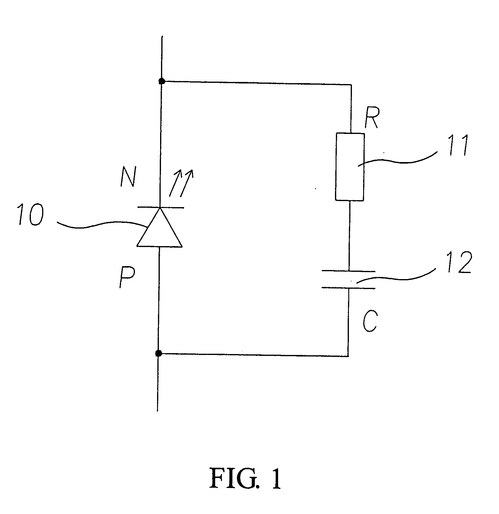
[0021]FIG. 1 is a circuit diagram showing an LED engaging a parallel connection with an RC circuit according to this invention, wherein a resistor 11 and a capacitor 12 in a series connection engages a parallel connection with an LED 10. The LED 10 is a high speed semiconductor, such as Groups III-V nitride semiconductors containing InGaN, which would easily induce ESD upon human contact thereby causing damages. The parallel connection of the LED with the circuit consisting of the resistor 11 and capacitor 12 connected in series guards the LED against damages. The laminar structure of the LED is illustrated in FIGS. 2 and 3 in details.
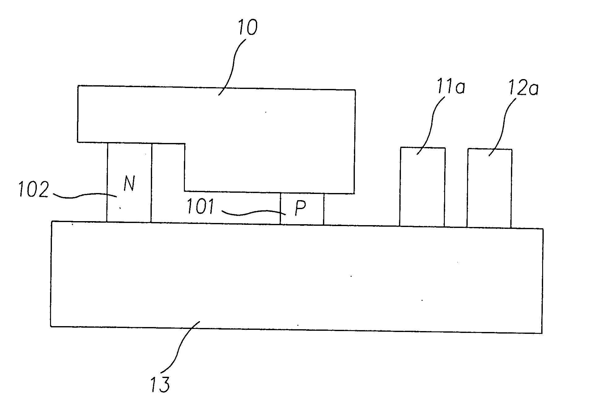
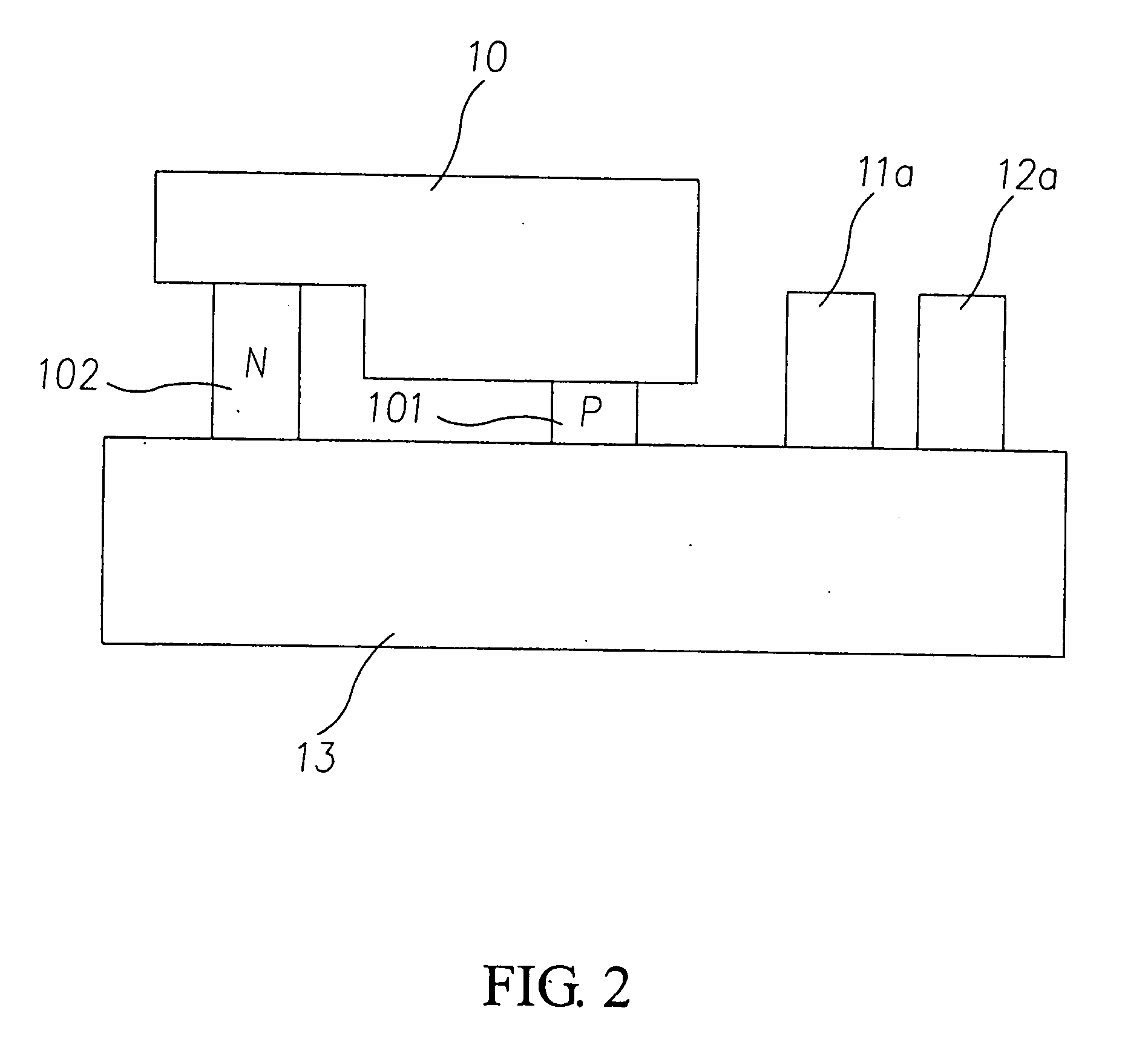
[0022]FIG. 2 is a schematic drawing illustrating the laminar structure of the LED in a parallel connection with the RC circuit according to an embodiment of this invention, wherein a resistor 11a and a capacitor 12a are situated outside a circuit substrate 13 and connected to a p-node 101 and an n-node 102 of the LED 10 via th...
second embodiment
[0026] [Second Embodiment]
[0027]FIGS. 4 and 5, respectively, illustrate a circuit diagram and a schematic drawing illustrating the laminar structure of an LED engaging a parallel connection with components of a first and a second ESD protection configuration according to this invention, comprising: an LED 20 having a junction formed by a p-node 201 and an n-node 202 and connected to a circuit substrate 23, the circuit substrate 23 having therein two p-type substrates 231 and one n-type substrate 232; a first ESD protection configuration 21 built-in the circuit substrate 23; and a second ESD protection configuration 22 built-in the circuit substrate 23.
[0028] The first ESD protection configuration 21 includes a first resistor 211, a third capacitor 212, and a first diode 213 that are connected in series and then engage a parallel connection with the LED 20. The first diode 213 has a p-node connected to the n-node 202 of the LED 20. The third capacitor 213 consists of a fifth capacit...
PUM
 Abstract
Description
Claims
Application Information
 - Generate Ideas
- Intellectual Property
- Life Sciences
- Materials
- Tech Scout
- Unparalleled Data Quality
- Higher Quality Content
- 60% Fewer Hallucinations
Browse by: Latest US Patents, China's latest patents, Technical Efficacy Thesaurus, Application Domain, Technology Topic, Popular Technical Reports.
© 2025 PatSnap. All rights reserved.Legal|Privacy policy|Modern Slavery Act Transparency Statement|Sitemap|About US| Contact US: help@patsnap.com