Semiconductor component having chip on board leadframe and method of fabrication

Inactive Publication Date: 2005-02-03
MICRON TECH INC
View PDF35 Cites 24 Cited by
  • Summary
  • Abstract
  • Description
  • Claims
  • Application Information

AI Technical Summary

Benefits of technology

[0010] The leadframe includes leadfingers having interconnect bonding sites for the wire interconnects, and terminal bonding sites for the terminal contacts. In addition, the terminal bonding sites can be arranged in an area array such as a grid array, edge array or peripheral array. The leadframe also includes bus bars whi

Problems solved by technology

However, one problem with metal lead frames occurs when wire bonded wires short to bus bars physically and electrically connecting different leadfingers o

Method used


Image

  • Semiconductor component having chip on board leadframe and method of fabrication
  • Semiconductor component having chip on board leadframe and method of fabrication
  • Semiconductor component having chip on board leadframe and method of fabrication

Examples


Embodiment Construction

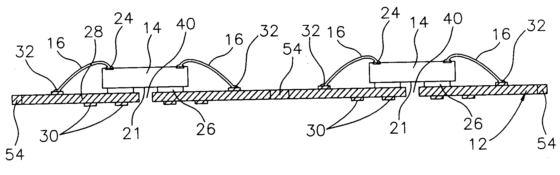
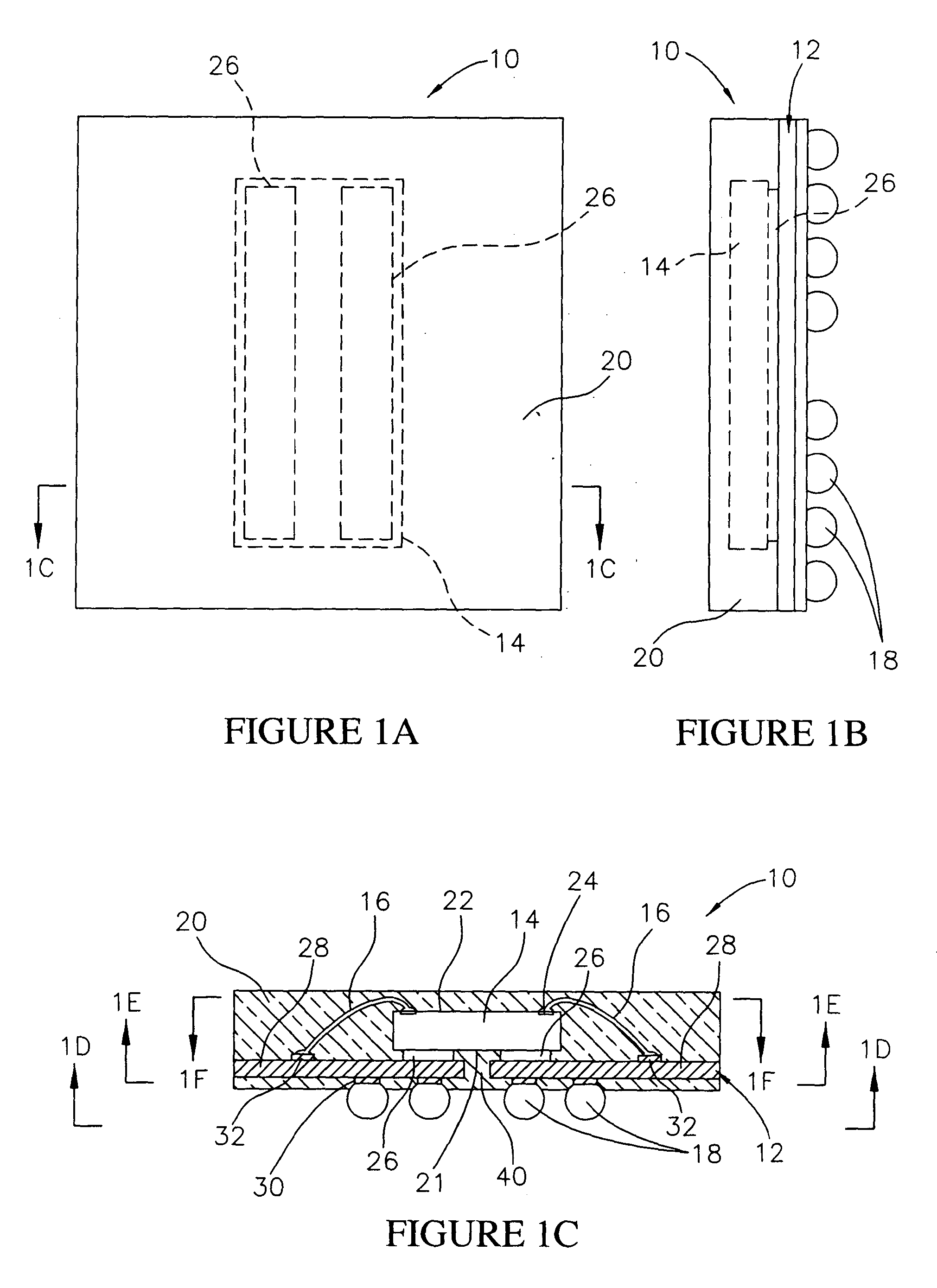
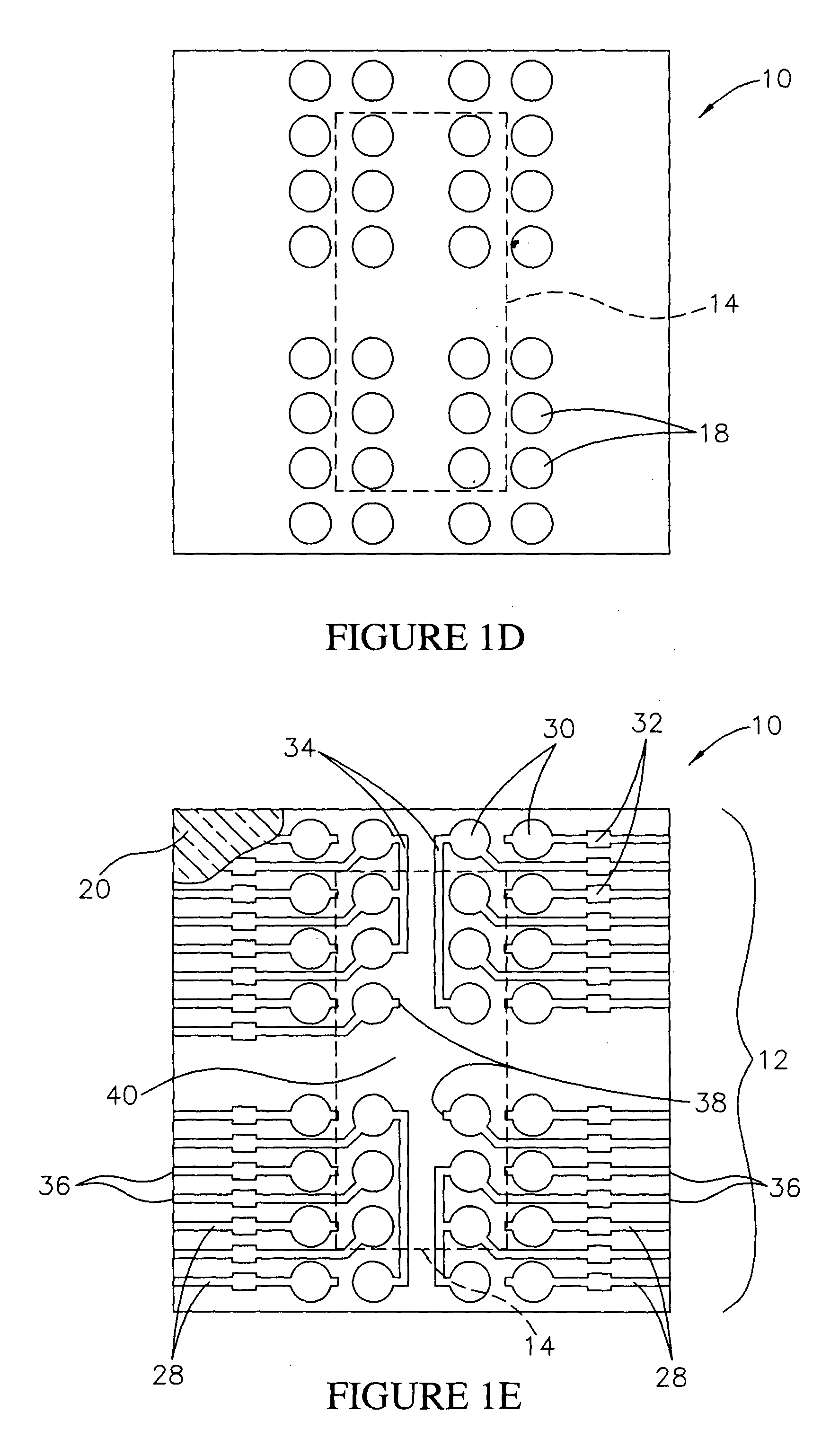
[0030] Referring to FIGS. 1A-1F, a semiconductor component 10 constructed in accordance with the invention is illustrated. As used herein, the term “semiconductor component” refers to an electronic element that includes a semiconductor die. Exemplary semiconductor components include semiconductor packages, semiconductor dice and BGA devices. In the illustrative embodiment the component 10 comprises a chip scale semiconductor package.

[0031] The component 10 includes a leadframe 12, a semiconductor die 14 back bonded to the leadframe 12, and wire interconnects 16 wire bonded to the die 14 and to the leadframe 12. The component 10 also includes an array of terminal contacts 18 attached to the leadframe 12, and an encapsulant 20 encapsulating the die 14, the wire interconnects 16 and the leadframe 12.

[0032] The die 14 can comprise a conventional semiconductor die having active semiconductor devices constructed in a desired electrical configuration. For example, the die 14 can comprise...


PUM


Abstract

A semiconductor component includes a chip on board leadframe, a semiconductor die back bonded and wire bonded to the leadframe, an encapsulant on the die and an area array of terminal contacts on the leadframe. The leadframe includes leadfingers, interconnect bonding sites for wire bonding the die, terminal bonding sites for the terminal contacts, and bus bars which electrically connect selected leadfingers to one another. The interconnect bonding sites are located on the leadframe relative to the bus bars such that shorting to the bus bars by wire interconnects is eliminated. A method for fabricating the component includes the steps of attaching the die to the leadframe, bonding the wire interconnects to the die and to the interconnect bonding sites, forming the encapsulant, and then forming the terminal contacts on the terminal bonding sites.

Description

FIELD OF THE INVENTION [0001] This invention relates generally to semiconductor manufacture and packaging. More particularly, this invention relates to a semiconductor component having a chip on board leadframe, to a method for fabricating the component, and to systems incorporating the component. BACKGROUND OF THE INVENTION [0002] Semiconductor components, such as packages and BGA devices, are being manufactured with a chip scale outline, and with a higher pin count than conventional plastic or ceramic components. Semiconductor components typically include a substrate, a semiconductor die, and terminal contacts, such as balls, bumps or pins, arranged in an area array, such as a ball grid array (BGA), or a pin grid array (PGA). Semiconductor components can also include an encapsulant which at least partially encapsulates the die and the substrate. [0003] Different methods are employed in the industry for fabricating semiconductor components. One conventional method uses a rigid subs...

Claims


Application Information

Patent Timeline
IPC IPC(8): H01L23/31H01L23/495
CPCH01L23/3107H01L2924/01322H01L23/4951H01L23/4952H01L24/32H01L24/45H01L24/48H01L24/50H01L24/86H01L24/97H01L2224/29007H01L2224/32014H01L2224/32245H01L2224/45124H01L2224/45144H01L2224/48091H01L2224/48247H01L2224/48465H01L2224/48599H01L2224/48699H01L2224/49171H01L2224/73265H01L2224/85424H01L2224/85444H01L2224/85447H01L2224/92247H01L2224/97H01L2924/01013H01L2924/01028H01L2924/01029H01L2924/01078H01L2924/01079H01L2924/01082H01L2924/014H01L2924/14H01L2924/1433H01L2924/15311H01L23/3128H01L2924/01033H01L2924/01005H01L2224/83805H01L24/49H01L24/29H01L2924/0132H01L2924/01012H01L2924/01014H01L2924/00014H01L2224/83H01L2224/85H01L2924/00H01L2924/01026H01L2224/48624H01L2224/48644H01L2224/48647H01L2224/48724H01L2224/48744H01L2224/48747H01L2924/12042H01L2924/181H01L2224/05554H01L2924/10161H01L2924/00012H01L23/495
Inventor KIM, DALSON YE SENGFOOK, JEFFREY TOH TUCKKUAN, LEE CHOON
Owner MICRON TECH INC
Why Eureka
Try Eureka