
MEMS Packaging Including Integrated Circuit Dies

a technology of integrated circuit dies and mems, which is applied in the field of microelectromechanical systems, can solve the problems of increasing signal latency and undesirable inductance, and achieve the effects of reducing rc delays and power consumption, reducing the footprint of mems packages, and increasing integration density

Inactive Publication Date: 2009-08-06
TAIWAN SEMICON MFG CO LTD
View PDF11 Cites 262 Cited by
  • Summary
  • Abstract
  • Description
  • Claims
  • Application Information

AI Technical Summary

Benefits of technology

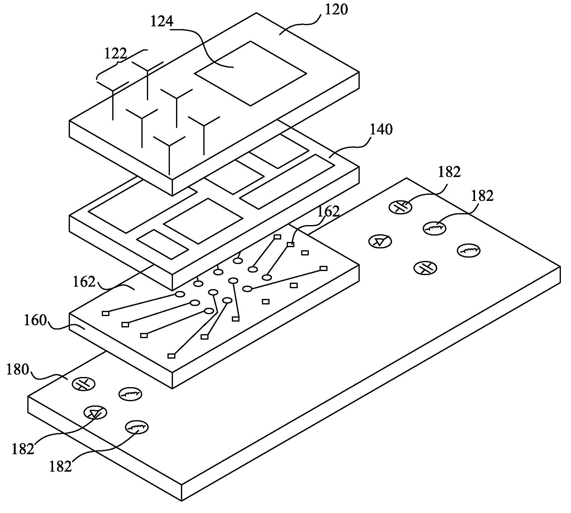
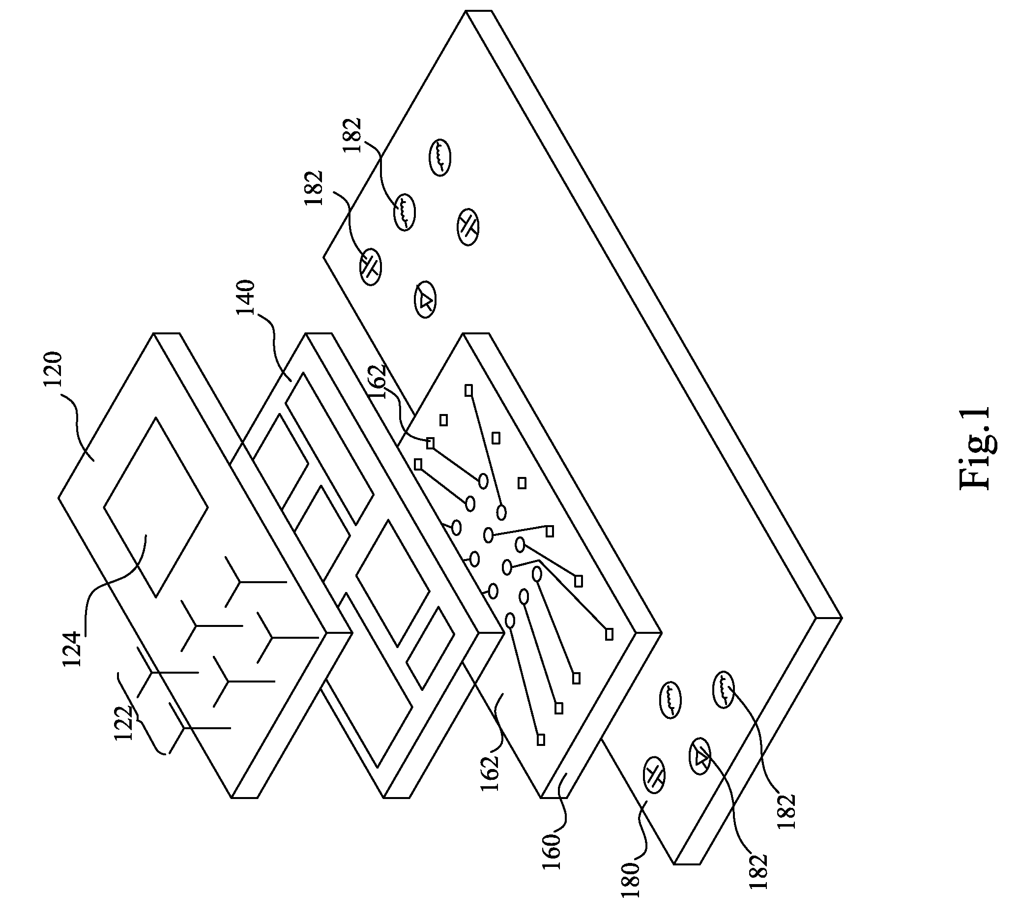
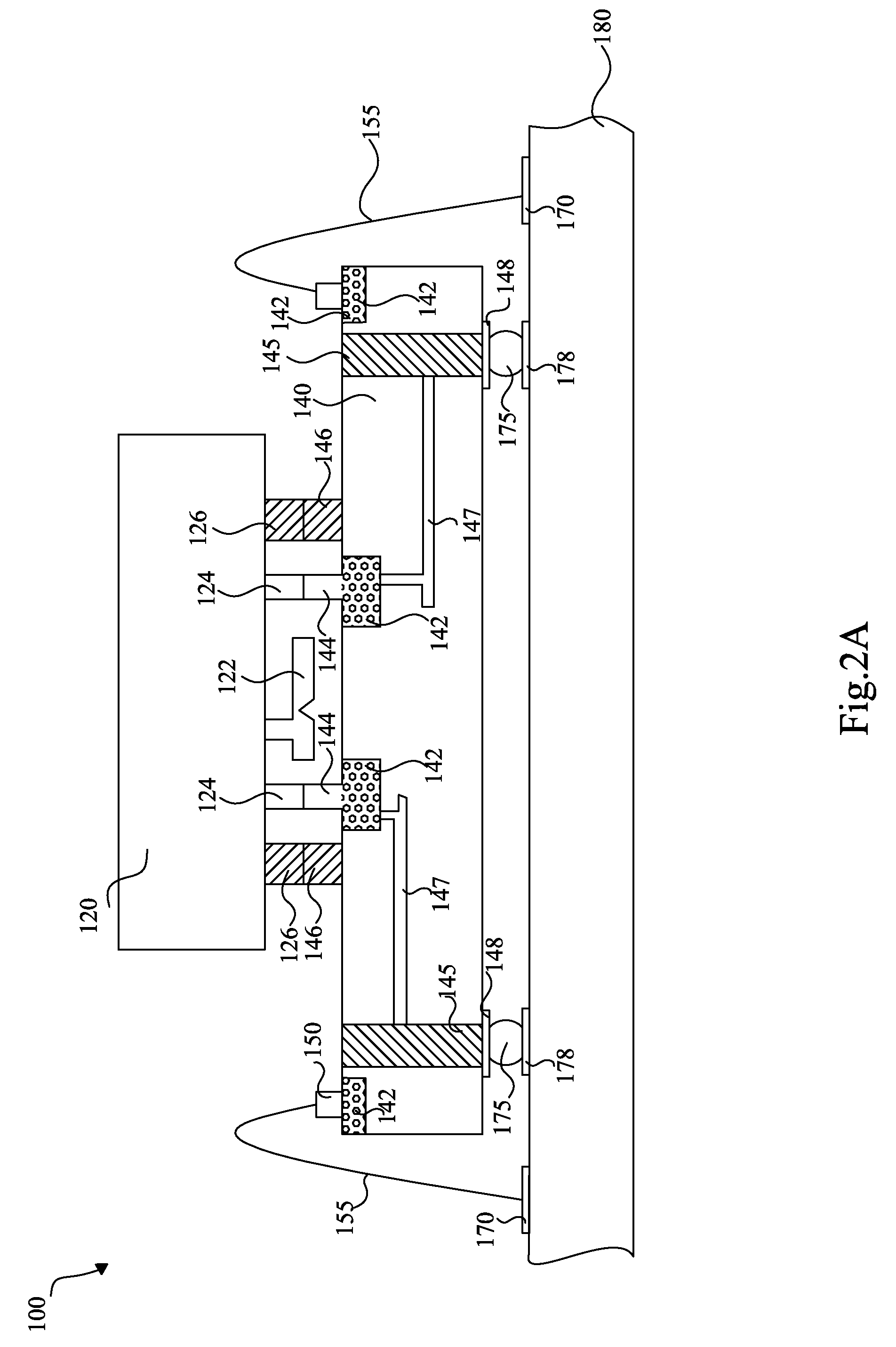
[0008]These and other problems are generally solved or circumvented, and technical advantages are generally achieved, by preferred embodiments of the present invention which provide MEMS packaging schemes that provide a system-on-package (SOP) configuration and a system-on-board (SOB) configuration. The MEMS package comprises one or more MEMS dies, a cap section having one or more integrated circuit (IC) dies, and a packaging substrate or a printed circuit board (PCB) arranged in a stacking manner. Vertical connectors, such as through-silicon-vias, are formed to provide short electrical connections between the various components. The MEMS packaging schemes enable higher integration density, reduced MEMS package footprint, reduced RC delays and power consumption.

Problems solved by technology

Among other drawbacks of an existing packaging approach, horizontal feed-throughs create crossing signal lines that may affect circuit performance, lengthy horizontal signal line routings may increase signal latency, and long metal traces may lead to undesirable inductance.

Method used


Image

  • MEMS Packaging Including Integrated Circuit Dies
  • MEMS Packaging Including Integrated Circuit Dies
  • MEMS Packaging Including Integrated Circuit Dies

Examples


Embodiment Construction

[0017]The making and using of the presently preferred embodiments are discussed in detail below. It should be appreciated, however, that the present invention provides many applicable inventive concepts that can be embodied in a wide variety of specific contexts. The specific embodiments discussed are merely illustrative of specific ways to make and use the invention, and do not limit the scope of the invention.

[0018]The present invention will be described with respect to preferred embodiments in a specific context, namely apparatus and method of integrating MEMS devices with multiple integrated circuit dies and / or other electronic components in a system-on-package (SOP) or system-on-board (SOB) configuration. However, features, structures or characteristics described according to the preferred embodiments may also be combined in suitable manners to form one or more other embodiments. Also, for clarification, the figures are drawn only to illustrate the relevant aspects of the inven...


PUM


Abstract

MEMS packaging schemes having a system-on-package (SOP) configuration and a system-on-board (SOB) configuration are provided. The MEMS package comprises one or more MEMS dies, a cap section having one or more integrated circuit (IC) dies, and a packaging substrate or a printed circuit board (PCB) arranged in a stacking manner. Vertical connectors, such as through-silicon-vias (TSVs), are formed to provide short electrical connections between the various components. The MEMS packaging schemes enable higher integration density, reduced MEMS package footprints, reduced RC delays and power consumption.

Description

[0001]This application claims the benefit of U.S. Provisional Application No. 61 / 025,174 filed on Jan. 31, 2008, entitled “Apparatus and Method for RF Integration,” which application is hereby incorporated herein by reference.TECHNICAL FIELD[0002]The present invention relates in general to micro-electromechanical system (MEMS) and more particularly to integrated MEMS devices with multiple integrated circuit dies in a system-on-package (SOP) or system-on-board (SOB) configuration.BACKGROUND[0003]A MEMS device is the integration of miniature mechanical elements, sensors, actuators, and electronics on a common silicon substrate through micro-fabrication technology. A sensor on a MEMS device typically includes a miniature moveable structure, such as a bridge, cantilevered beam, suspended mass, membrane or capacitive element device. A sensor may gather information from the environment through measuring mechanical, thermal, biological, chemical, optical, and / or magnetic phenomena. The ele...

Claims


Application Information

Patent Timeline
Patent Type & Authority Applications(United States)
IPC IPC(8): H01L29/84H01L23/04
CPCB81C1/0023B81C1/00238H01L2224/48091H01L2224/73257H01L2924/19107H01L2924/1461H01L2924/00014H01L2924/00B81C2203/0792
Inventor CHUNG, SHINEHSUEH, FU-LUNG
Owner TAIWAN SEMICON MFG CO LTD
Learn More