

Substrate with reinforced contact pad structure
a contact pad and substrate technology, applied in the direction of printed circuit aspects, sustainable manufacturing/processing, final product manufacturing, etc., can solve the problems of poor adhesion or even failure, low assembly yield, traces b>30/b> to break or electrically fail, etc., to achieve the effect of greatly enhancing the connection strength between the trace 130 and the nsmd type contact pad 120, greatly enhancing the position stability and reliability of the nsmd type contact pad
- Summary
- Abstract
- Description
- Claims
- Application Information
AI Technical Summary
Benefits of technology
Problems solved by technology
Method used
Image

Examples
Embodiment Construction
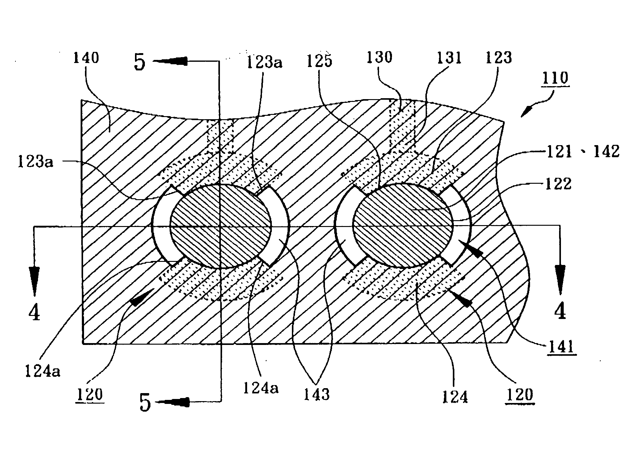
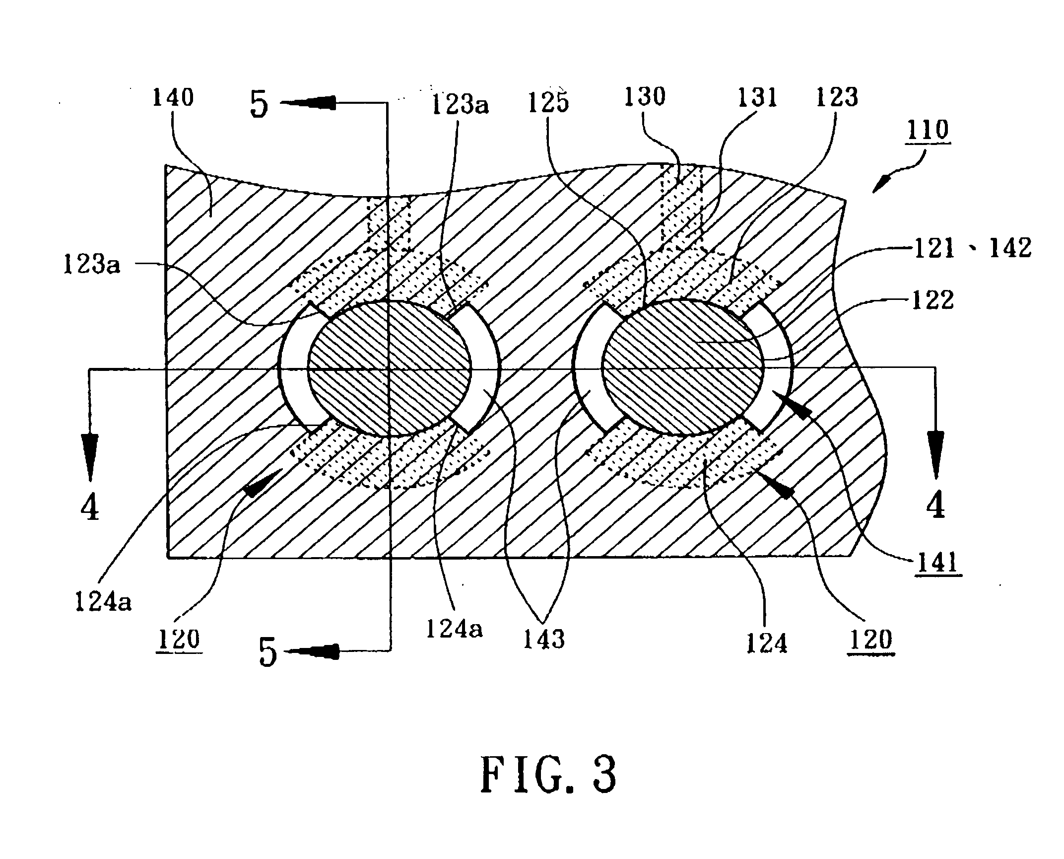
[0014] Please refer to the drawings attached, the present invention will be described by means of an embodiment below. According to an embodiment of the present invention, a substrate with reinforced contact pad structure is shown in FIGS. 3, 4, and 5. It mainly comprises a substrate 110, a metal wiring layer, and a solder mask 140. The metal wiring layer includes at least a contact pad 120, a trace 130, and at least a first extension 123. As shown in FIG. 6, the first extension 123 connects the contact pad 120 and the trace 130. The substrate 110 comprises a resin layer with circuits design, not shown in the figures. The substrate 110 has a surface 111 for SMT connection.
[0015] Referring to FIG. 4 and 5, the metal wiring layer including the contact pad 120, the trace 130 and first extension 123 is disposed on the surface 111 of the substrate 110. Referring to FIG. 4 and 6, the contact pad 120 has a bonding surface 121 and a sidewall 122. There is a V-shaped indentation between the...
PUM
 Abstract
Description
Claims
Application Information