
Semiconductor device

Inactive Publication Date: 2005-02-10
SEMICON COMPONENTS IND LLC
View PDF9 Cites 9 Cited by
  • Summary
  • Abstract
  • Description
  • Claims
  • Application Information

AI Technical Summary

Benefits of technology

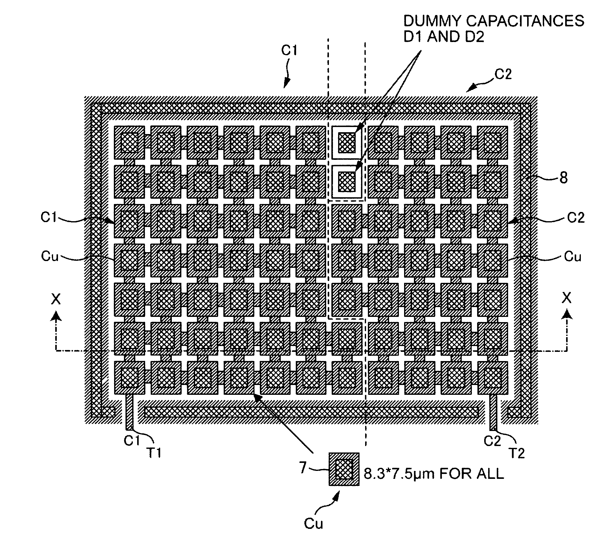
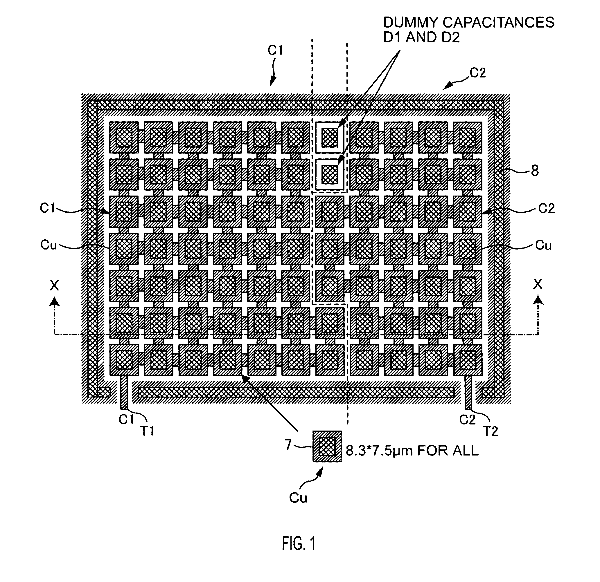
[0014] It is therefore unnecessary to route the lead-out electrode for each of the unit capacitive elements, allowing downsizing of the semiconductor device through area reduction of the capacitive element group and providing improved patterning accuracy as a result of easier patterning. This in turn leads to improved accuracy in capacitance ratio.
[0015] The at least one lead-out electrode is provided so as to surround the top electrodes as a whole of the capacitive element group. This ensures further reduction of the capacitive element group in area. Since the lead-out electrode is provided so as to surround the top electrodes as a whole, the connection of the lead-out electrode with external and other circuitry is facilitated.
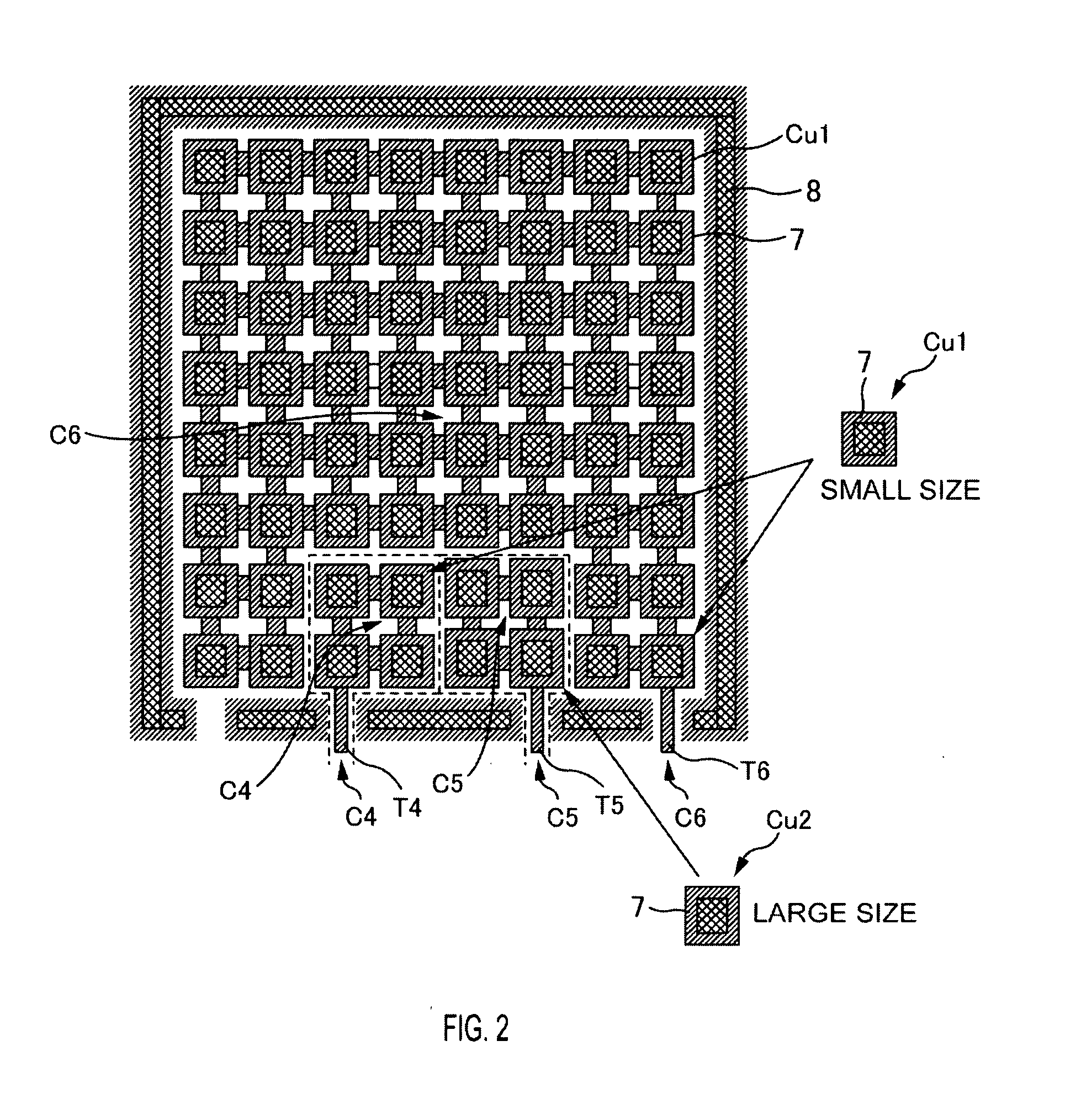
[0016] Further, the unit capacitive elements can be identical at least in each of the at least one capacitive element group. Identicalness of the unit capacitive elements ensures enhanced patterning accuracy, thus providing improved accuracy of capacitance ratio.
[0018] The unit capacitive elements are arranged in grid form, with the top electrodes of the unit capacitive elements adjacent to each other joined together in each of the at least one capacitive element group. This eliminates the need to form a wiring pattern for drawing out the top electrode 7 outwards for each of the unit capacitive elements Cu, making it possible to mount the unit capacitive elements at high density and thereby ensuring further reduction of the capacitive element groups in area. This leads to further downsizing of the semiconductor device. Arrangement of the unit capacitive elements in grid form provides improved patterning accuracy, thus ensuring improved accuracy in capacitance ratio.
[0020] Further, a plurality of the capacitive element groups are formed in the semiconductor device, and there is provided at least one lead-out electrode for the bottom electrodes of the unit capacitive elements of the plurality of capacitive element groups along a circumference going around the top electrodes as a whole of the plurality of capacitive element groups. This eliminates the need to provide the lead-out electrode for each of the capacitive element groups, allowing reduction in area of the plurality of capacitive element groups as a whole. This leads to downsizing of the semiconductor device provided with a plurality of capacitive element groups.
[0022] This prevents generation of steps as a result of no elements existing in the vacant region, thus facilitating patterning and providing improved patterning accuracy. This in turn leads to improved accuracy in capacitance ratio.

Problems solved by technology

Configuring the above capacitive element groups Ca and Cb presents problems in layout pattern of the unit capacitive elements Cy.
In general, however, the smaller the capacitance value of the unit capacitive element Cy for smaller area, the poorer the accuracy of the capacitance value and capacitance ratio.
The aforementioned prior-art layout method shown in FIG. 7, however, has been unfit for downsizing.

Method used


Image

  • Semiconductor device
  • Semiconductor device
  • Semiconductor device

Examples


Embodiment Construction

[0033] In FIGS. 1 to 5, the same reference numerals are assigned to components equivalent or identical to conventional components shown in the sectional view of FIG. 6, with their description substituted by the description of the aforementioned related art technology.

[0034] As shown in the plan view of FIG. 1, the semiconductor device has a pair of capacitive element groups C1 and C2. The left side demarcated by a dashed line is a region of the capacitive element group C1, whereas the right side thereof is a region of the capacitive element group C2. It is to be noted that dummy elements D1 and D2, that will be described later, are provided in a region enclosed by two that the dashed line is split into at the upper portion.

[0035] The capacitive element groups C1 and C2 are configured by arranging a number of identical unit capacitive elements Cu. Then, there is provided the lead-out electrode 8 of the bottom electrode of the unit capacitive elements Cu of the capacitive element gr...


PUM


Abstract

There is disclosed a semiconductor device comprising at least one capacitive element group having a plurality of unit capacitive elements. At least one lead-out electrode for bottom electrodes of the unit capacitive elements of the capacitive element group is provided along a circumference going around top electrodes as a whole of the capacitive element group. The at least one lead-out electrode is provided so as to surround the top electrodes as a whole of the capacitive element group.

Description

NOTICE OF COPYRIGHTS AND TRADE DRESS [0001] A portion of the disclosure of this patent document contains material which is subject to copyright protection. This patent document may show and / or describe matter which is or may become trade dress of the owner. The copyright and trade dress owner has no objection to the facsimile reproduction by any one of the patent disclosure as it appears in the Patent and Trademark Office patent files or records, but otherwise reserves all copyright and trade dress rights whatsoever. RELATED APPLICATION INFORMATION [0002] The present application claims priority upon Japanese Patent Application No. 2003-197067 filed on Jul. 15, 2003, which is herein incorporated by reference. BACKGROUND OF THE INVENTION [0003] 1. Field of the Invention [0004] The present invention relates to a semiconductor device. [0005] 2. Description of the Related Art [0006] A semiconductor device is known that incorporates a plurality of capacitive elements. Such a semiconductor...

Claims


Application Information

Patent Timeline
IPC IPC(8): H01L27/04H01L21/822H01L27/08H01L29/94
CPCH01L29/94H01L27/0805H01L27/04
Inventor KANEKO, SATORU
Owner SEMICON COMPONENTS IND LLC
Learn More