Plasma display panel

a technology of display panel and plasma, which is applied in the direction of gas discharge electrode, gas discharge electrode, sustain/scan electrode, etc., can solve the problems of non-uniform brightness characteristics, significant voltage requirements, and each discharge cell, and achieve the effect of improving discharge efficiency

Inactive Publication Date: 2005-02-10
SAMSUNG SDI CO LTD
View PDF34 Cites 39 Cited by
  • Summary
  • Abstract
  • Description
  • Claims
  • Application Information

AI Technical Summary

Benefits of technology

[0014] In exemplary embodiments accordance with the present invention, a plasma display panel is provided in which the formation

Problems solved by technology

However, the discharge sustain electrodes structured as described above are not made with the goal of optimizing discharge characteristics between discharge cells.
Also, since the spaces between the transparent electrodes are large, a significant voltage is required.
As a result, non-uniform brightness characteristics r

Method used


Image

  • Plasma display panel
  • Plasma display panel
  • Plasma display panel

Examples


Embodiment Construction

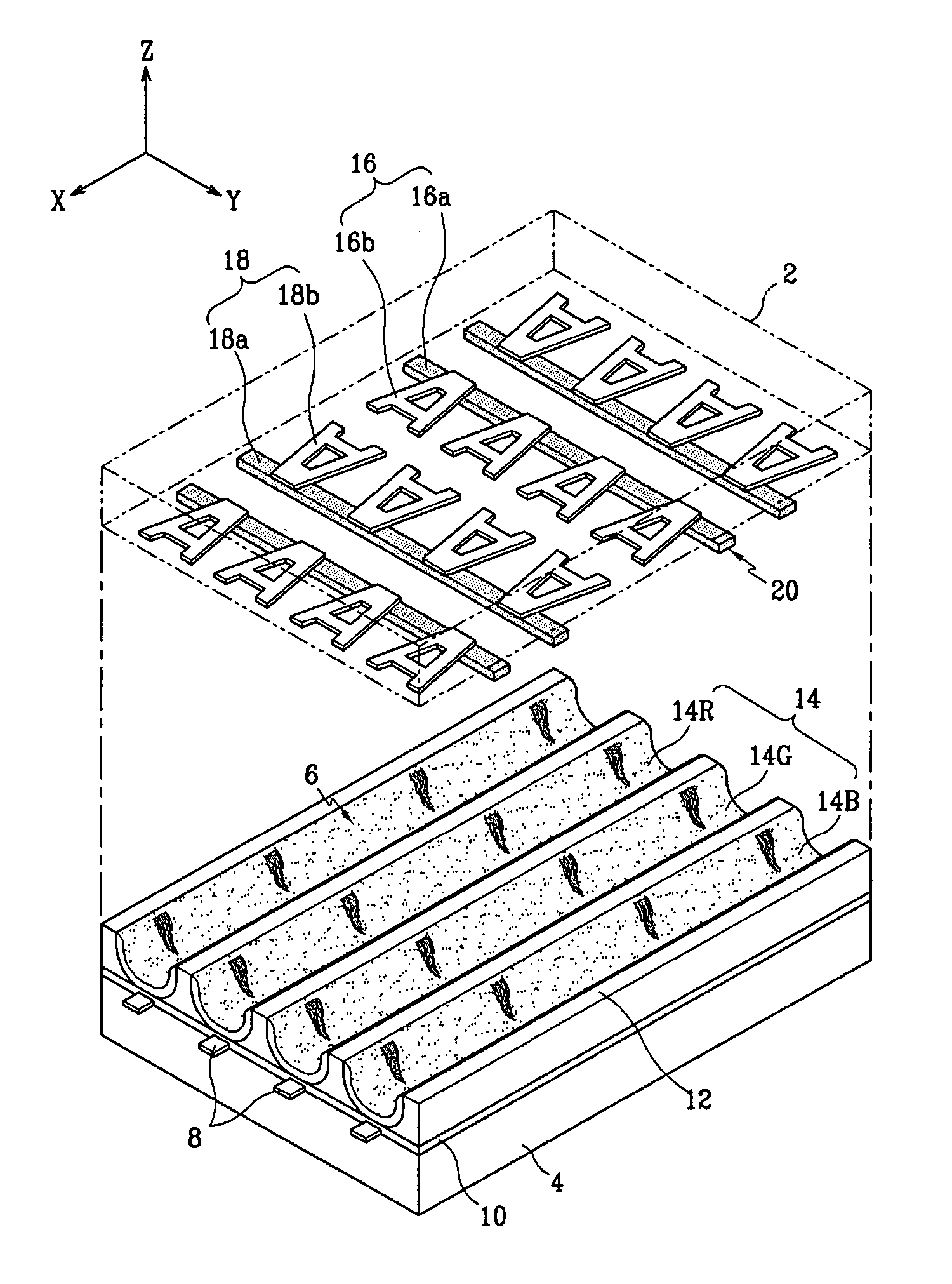
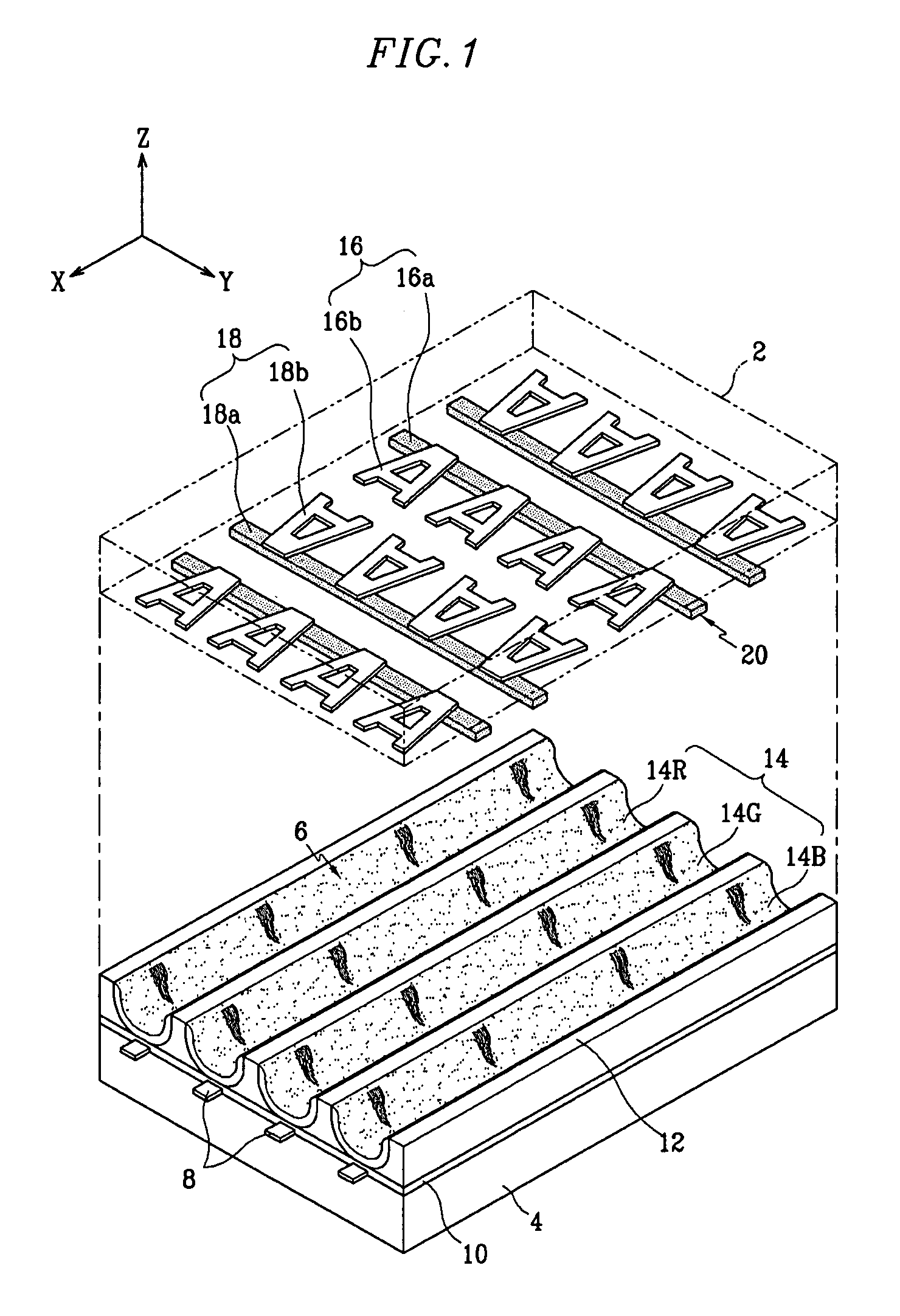
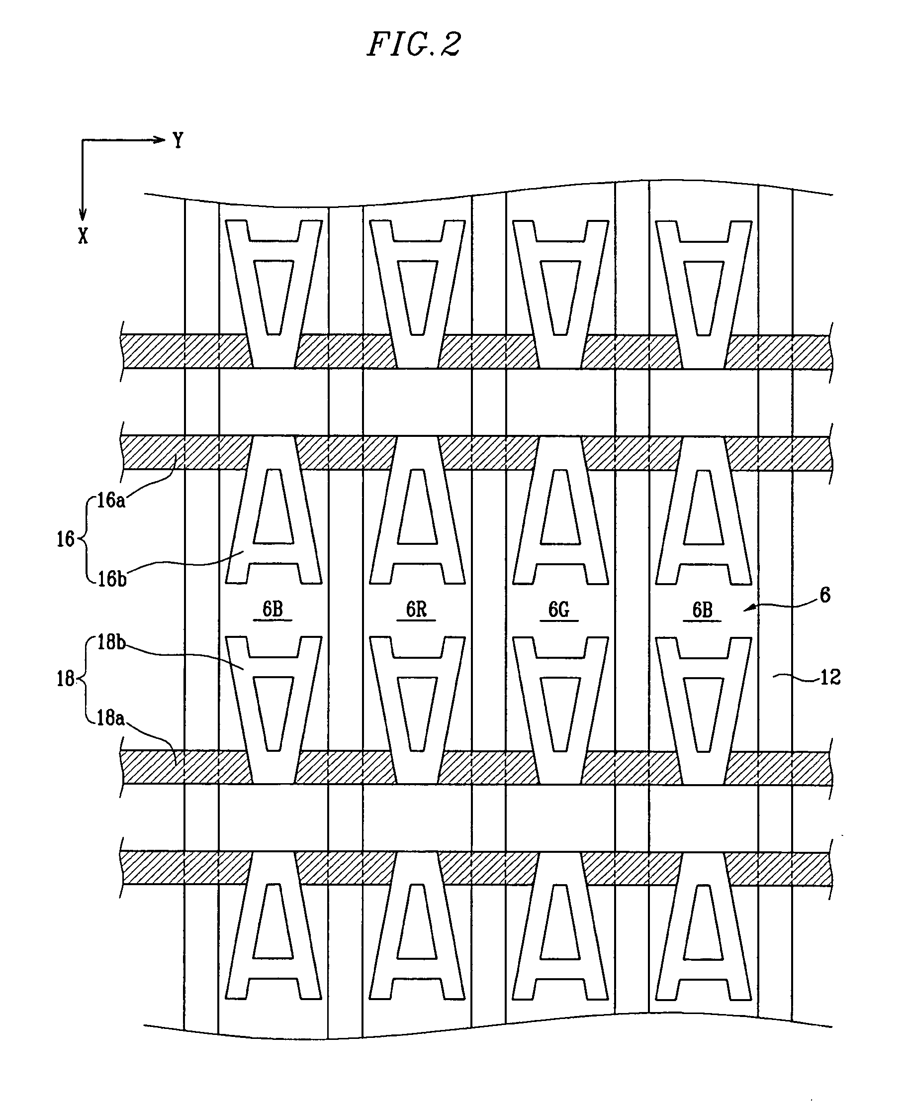
[0034]FIG. 1 is a partial exploded perspective view of a plasma display panel (PDP) according to a first exemplary embodiment of the present invention, and FIG. 2 is a partial plan view of the PDP of FIG. 1.

[0035] A PDP according to the first exemplary embodiment includes first substrate 2 and second substrate 4 provided substantially in parallel with a predetermined gap therebetween. Discharge cells 6 are formed between first and second substrates 2 and 4. Independent discharge taking place in each of the discharge cells 6 results in the emission of visible light for the display of color images.

[0036] In more detail, address electrodes 8 are formed along one direction (direction X in the drawings) on a surface of second substrate 4 opposing first substrate 2. Dielectric layer 10 is formed over an entire surface of second substrate 4 covering address electrodes 8. Address electrodes 8 are formed in a uniform, stripe pattern with a predetermined interval therebetween.

[0037] Barrie...


PUM


Abstract

A plasma display panel. A first substrate and a second substrate are provided opposing one another with a predetermined gap therebetween. Address electrodes are formed on the second substrate. Barrier ribs are mounted between the first substrate and the second substrate defining a plurality of discharge cells. Phosphor layers are formed within the discharge cells. Discharge sustain electrodes are formed on the first substrate. The discharge sustain electrodes include bus electrodes that extend such that a pair of the bus electrodes is provided for each of the discharge cells, and protrusion electrodes extending from each of the bus electrodes such that a pair of opposing protrusion electrodes is formed within an area corresponding to each discharge cell. A distal end of each protrusion electrode includes an indentation such that a gap is formed between the pair of opposing protrusion electrodes, and an aperture is formed in each protrusion electrode.

Description

CROSS REFERENCE TO RELATED APPLICATIONS [0001] This application claims priority to and the benefit of Korean Patent Application No. 2003-0045199 filed on Jul. 4, 2003, Korean Patent Application No. 2003-0050278 filed on Jul. 22, 2003, Korean Application No. 2003-0052598 filed on Jul. 30, 2003 and Korean Application No. 2003-0053461 filed on Aug. 1, 2003, in the Korean Intellectual Property Office, the entire contents of all of which are incorporated herein by reference. BACKGROUND OF THE INVENTION [0002] (a) Field of the Invention [0003] The present invention relates to a plasma display panel (PDP), and more particularly, to a plasma display panel in which the formation of discharge sustain electrodes is improved to thereby enhance discharge efficiency. [0004] (b) Description of the Related Art [0005] A PDP is a display device that uses vacuum ultraviolet rays generated by gas discharge in discharge cells to excite phosphors, thereby realizing the display of images. With its ability...

Claims


Application Information

Patent Timeline
IPC IPC(8): H01J17/04H01J17/49
CPCH01J11/12H01J11/24H01J2211/365H01J2211/245H01J2211/323H01J11/32
Inventor WOO, SEOK-GYUNKANG, TAE-KYOUNGKIM, WOO-TAEKANG, KYOUNG-DOOYOO, HUN-SUKKWON, JAE-IK
Owner SAMSUNG SDI CO LTD
Why Eureka
Try Eureka