Method of dividing a plate-like workpiece

a workpiece and plate-like technology, applied in metal working equipment, manufacturing tools, welding/soldering/cutting articles, etc., can solve the problems of low-k film falling off, burr formation, semiconductor chip damage, etc., and achieve high accuracy

Inactive Publication Date: 2005-02-17
DISCO CORP
View PDF7 Cites 33 Cited by
  • Summary
  • Abstract
  • Description
  • Claims
  • Application Information

AI Technical Summary

Benefits of technology

[0011] According to the present invention, since the length between the outer sides of grooves on both sides formed in the laser beam application step is set to be larger than the thickness of the cutting blade, and the cutting b...

Problems solved by technology

As the Low-k film consists of multi-layers (5 to 15 layers) like mica and is extremely fragile, when the semiconductor wafer having the above Low-k film laminated thereon is cut along a dividing line with a cutting blade, a problem occurs that the Low-k film falls off, and this falling-off reaches a circuit and causes a fatal damage to a semiconductor chip.
When the semiconductor wafer having a metal patter...

Method used


Image

  • Method of dividing a plate-like workpiece
  • Method of dividing a plate-like workpiece
  • Method of dividing a plate-like workpiece

Examples


first embodiment

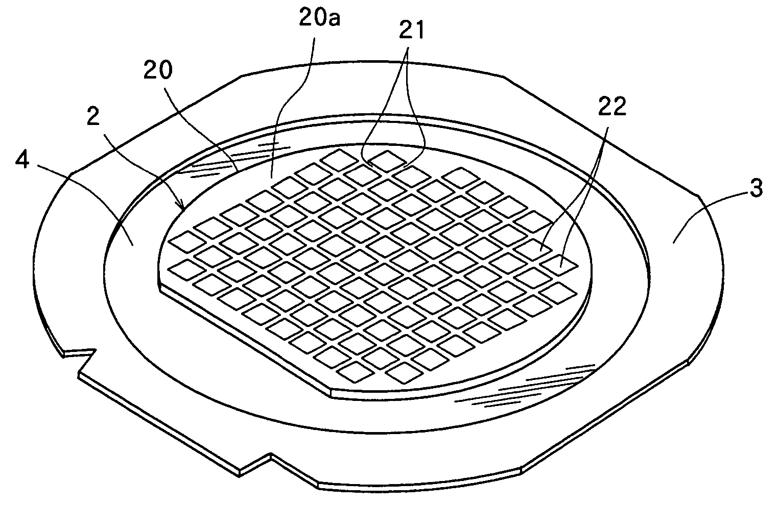
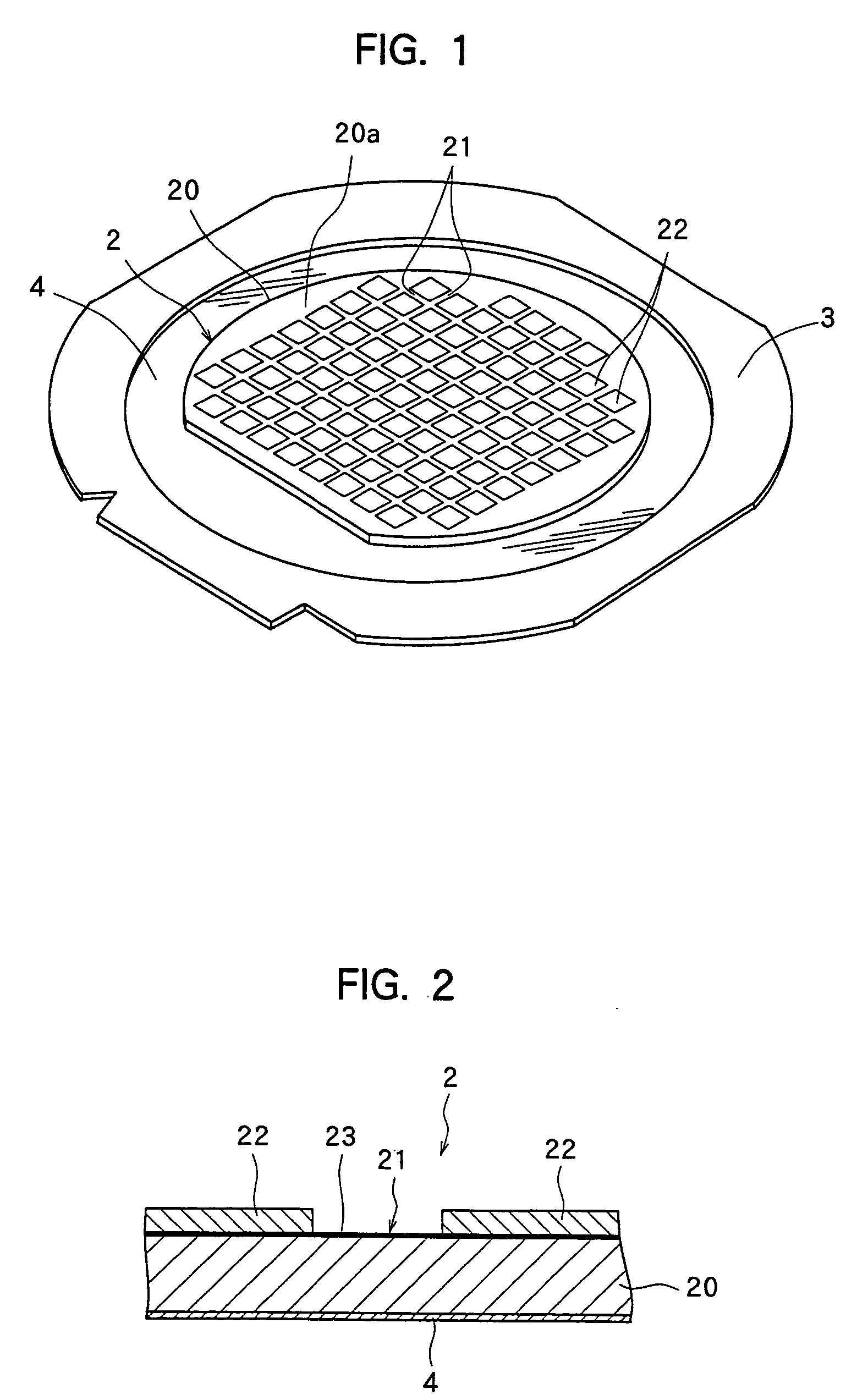
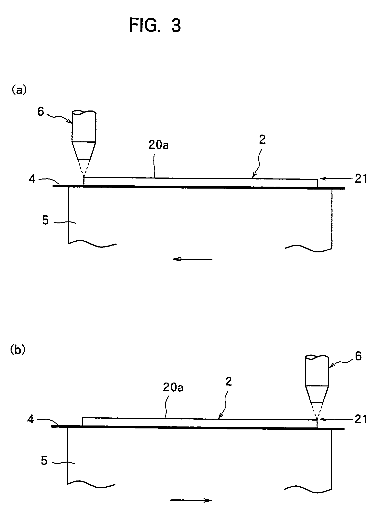
[0024] The method of manufacturing semiconductor chips by dividing the above semiconductor wafer 2 into individual semiconductor chips according to the present invention will be described with reference to FIGS. 3 to 6.

[0025] In the method of dividing a plate-like workpiece according to the present invention, the laser beam application step for applying a laser beam along the dividing lines 21 formed on the semiconductor wafer 2 to form grooves deeper than the layer of the Low-k film 23 in the dividing lines 21 is first carried out. That is, as shown in FIGS. 3(a) and 3(b), the semiconductor wafer 2 is placed on the chuck table 5 of a laser beam processing machine in such a manner that its front surface 20a faces up and held on the chuck table 5 by a suction means that is not shown. Thereafter, the chuck table 5 holding the semiconductor wafer 2 is moved to a laser beam processing start position of a laser beam processing area. At this moment, as shown in FIG. 3(a), the semiconducto...

second embodiment

[0046] A description is subsequently given of the method of dividing a plate-like workpiece according to the present invention with reference to FIGS. 7(a) and 7(b) and FIGS. 8(a) and 8(b).

[0047] In the second embodiment, the laser beam application step is the same as that of the first embodiment and the cutting step differs from that of the first embodiment. That is, in the second embodiment, the cutting step is divided into a first cutting substep and a second cutting substep.

[0048] In the first cutting substep, the semiconductor wafer 2 having two grooves 21b and 21b that have been formed deeper than the layer of the Low-k film 23 in all the dividing lines 21 in the laser beam application step as shown in FIG. 4 is placed and held on the chuck table 7 in such a manner that its front surface 20a faces up as shown in FIG. 5(a), like the above first embodiment. Then, as shown in FIG. 5(a), the chuck table 7 holding the semiconductor wafer 2 is moved to the cutting start position of...

third embodiment

[0051] A description is subsequently given of the method of dividing a plate-like workpiece according to the present invention with reference to FIGS. 9(a) to 9(c).

[0052] In the third embodiment, as shown in FIG. 9(a), two grooves 21c and 21c are formed in the dividing lines 21 of the semiconductor wafer 2 in the laser beam application step in such a manner that their inner sides overlap with each other to remove the Low-k film 23 in the cutting area with a cutting blade later described. The width of the cutting area from which the Low-k film 23 has been removed is set to be larger than the thickness of the cutting blade.

[0053] After the laser beam application step is carried out as described above, the same cutting step as in the first embodiment is carried out. That is, as shown in FIG. 9(b), the cutting blade 8 having a thickness of 20 μm, for example, is positioned at the center in the width direction of the grooves 21c and 21c and the lower end of the cutting blade 8 is positi...


PUM

PropertyMeasurementUnit
Thicknessaaaaaaaaaa
Areaaaaaaaaaaa

Abstract

A method of dividing a plate-like workpiece having a layer that is made of a different material from that of a substrate and is formed on the front surface of the substrate along predetermined dividing lines, comprising a laser beam application step for applying a laser beam along the dividing lines formed on the plate-like workpiece to form a plurality of grooves deeper than the layer and a cutting step for cutting the plate-like workpiece with a cutting blade along the plurality of grooves formed in the laser beam application step, wherein a length between the outer sides of grooves on both sides formed in the laser beam application step is set to be larger than the thickness of the cutting blade and the cutting blade cuts the area between the outer sides of the grooves on both sides in the cutting step.

Description

FIELD OF THE INVENTION [0001] The present invention relates to a method of dividing a plate-like workpiece such as a semiconductor wafer or the like. More specifically, it relates to a method of dividing a plate-like workpiece having a layer that is made of a different material from that of a substrate and is formed on the front surface of the substrate, along predetermined dividing lines. DESCRIPTION OF THE PRIOR ART [0002] As is known to people of ordinary skill in the art, in the production process of semiconductor devices, individual semiconductor chips are manufactured by forming a circuit such as IC or LSI in a plurality of areas sectioned by dividing lines called “streets” formed in a lattice pattern on the front surface of a substantially disk-like semiconductor wafer and cutting the semiconductor wafer along the dividing lines to divide it into the circuit-formed areas. Cutting along the dividing lines of the semiconductor wafer is generally carried out by a cutting machine...

Claims


Application Information

Patent Timeline
IPC IPC(8): B23K26/40H01L21/301B28D5/02
CPCB23K26/4075B28D5/022B23K2201/40B23K26/40B23K2101/40B23K2103/50
Inventor GENDA, SATOSHI
Owner DISCO CORP
Why Eureka
Try Eureka