

Apparatus and method to reduce signal cross-talk
a technology of electromagnetic interference and signal cross-talk, applied in the field of electromagnetic interference interference, can solve the problems of increasing the size of the package, and achieve the effects of reducing cross-talk, increasing the size of the package, and reducing the cross-talk
- Summary
- Abstract
- Description
- Claims
- Application Information
AI Technical Summary
Benefits of technology
Problems solved by technology
Method used
Image

Examples
Embodiment Construction
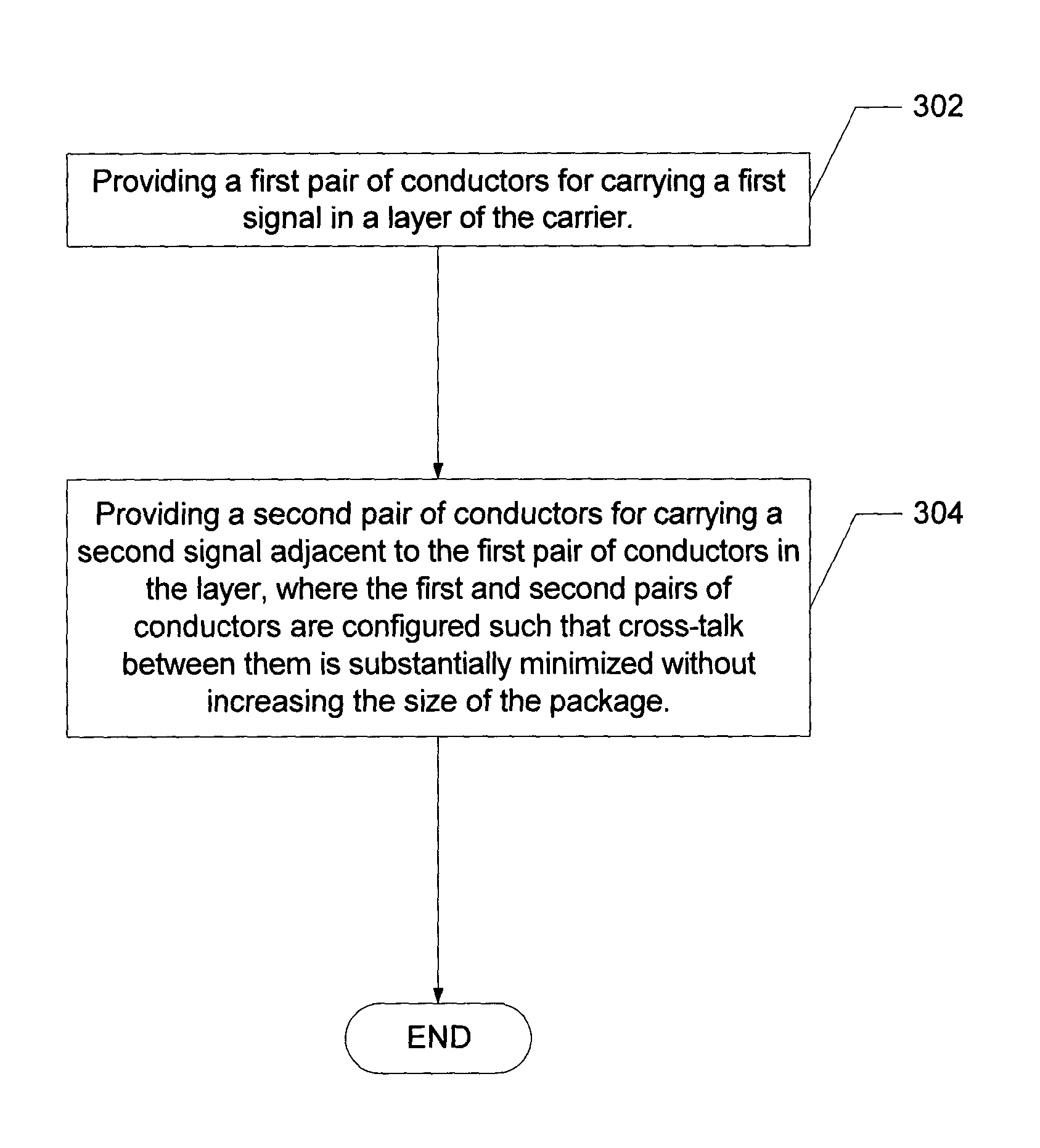
[0020] The present invention provides an improved apparatus and method for reducing cross-talk between adjacent signals in a layer of a semiconductor chip package. The following description is presented to enable one of ordinary skill in the art to make and use the invention and is provided in the context of a patent application and its requirements. Various modifications to the preferred embodiment will be readily apparent to those skilled in the art and the generic principles herein may be applied to other embodiments. Thus, the present invention is not intended to be limited to the embodiment shown but is to be accorded the widest scope consistent with the principles and features described herein.
[0021] To more particularly describe the features of the present invention, please refer to FIGS. 3 through 8 in conjunction with the discussion below.
[0022]FIG. 3 is a flowchart illustrating a preferred embodiment of a method for reducing cross-talk between adjacent signals in a layer...
PUM
 Abstract
Description
Claims
Application Information