Display device employing light control member and display device manufacturing method

a technology of light control member and display device, which is applied in the direction of instruments, non-linear optics, optics, etc., can solve problems such as unclear display images

Inactive Publication Date: 2005-02-24
CITIZEN WATCH CO LTD
View PDF3 Cites 80 Cited by
  • Summary
  • Abstract
  • Description
  • Claims
  • Application Information

AI Technical Summary

Benefits of technology

[0027] According to the fourteenth aspect, in the display device according to the first aspect, the display cell has a liquid crystal sealed between the first and

Problems solved by technology

Furthermore, the same problem occurs even when the adhesive is applied at an incorrect position on the light control member.
Moreover, even if the position of the light control member on the first transparent sub

Method used


Image

  • Display device employing light control member and display device manufacturing method
  • Display device employing light control member and display device manufacturing method
  • Display device employing light control member and display device manufacturing method

Examples


first embodiment

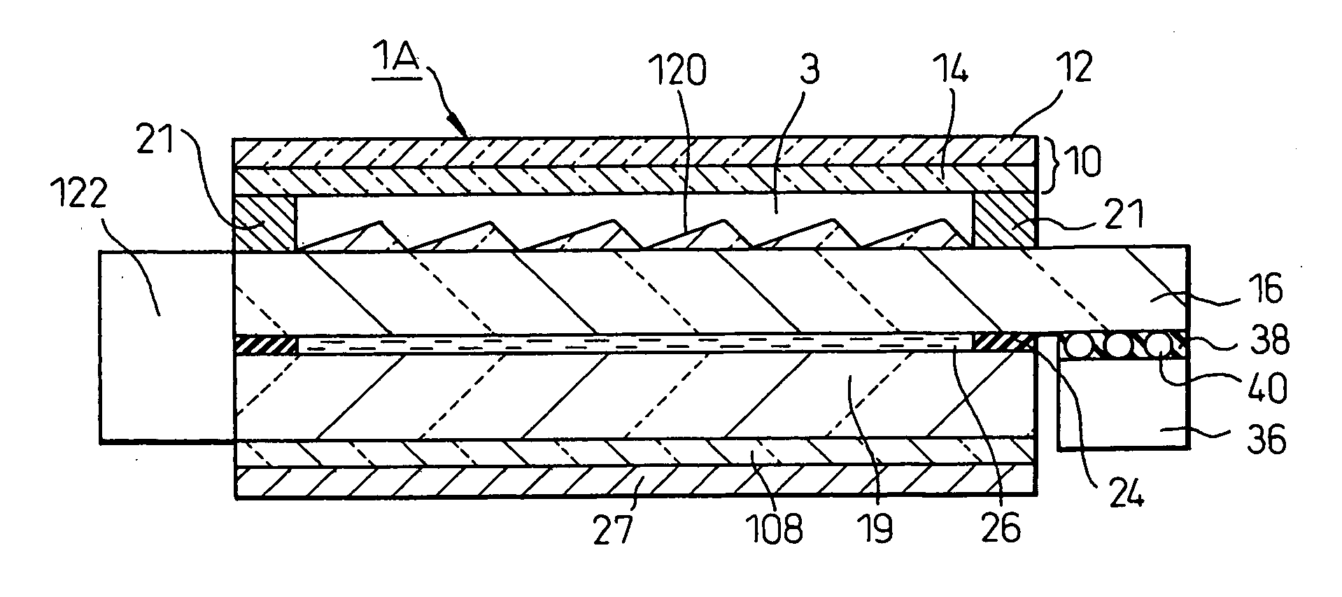
[0124]FIG. 17A shows the structure of a liquid crystal display device 2A in accordance with a first embodiment that is manufactured using a first transparent substrate 16 having a light control member 120 formed thereon according to the manufacturing method shown in FIG. 16A to FIG. 16E, and that includes a reflective layer 27 in a liquid crystal cell thereof. A second transparent substrate 19 is superposed on the side of the first transparent substrate 16 where an electrode (not shown) is provided, with a liquid crystal layer 26 and the reflective layer 27 between them, whereby a liquid crystal cell is produced. The liquid crystal layer 26 is sealed with a sealing member 24 and has a thickness of about 5 μm. In the present embodiment, the second transparent substrate 19 is thinner than the first transparent substrate 16. The thickness of the second transparent substrate 19 may be level with that of the first transparent substrate 16 as it is in the aforesaid examples of liquid crys...

second embodiment

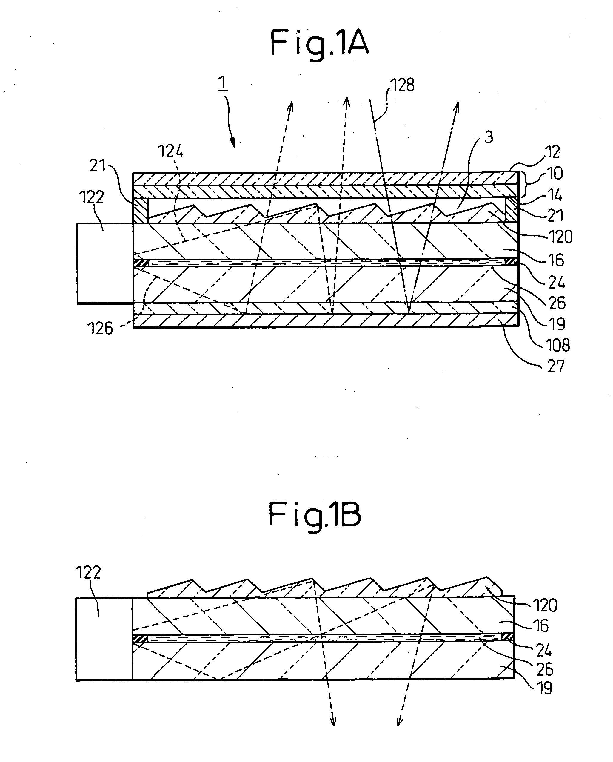
[0127]FIG. 17B shows a liquid crystal display device 2B in accordance with a second embodiment that is manufactured using a first transparent substrate 16 or a component having a light control member 120 formed thereon according to the manufacturing method shown in FIG. 16A to FIG. 16E, and that includes a reflective layer 27 in a liquid crystal cell thereof. A second transparent substrate 19 is superposed on the side of the first transparent substrate 16 where an electrode (not shown) is provided, with a liquid crystal layer 26 and the reflective layer 27 between them, whereby the liquid crystal cell is produced. The liquid crystal layer 26 is sealed with a sealing member 24 and has a thickness of about 5 μm.

[0128] A difference of the liquid crystal display device 2B from the liquid crystal display device 2A lies in the shape of the light control member 120. In the liquid crystal display device 2A, the continuous triangular cross-sectional shape of the light control member 120 is t...

third embodiment

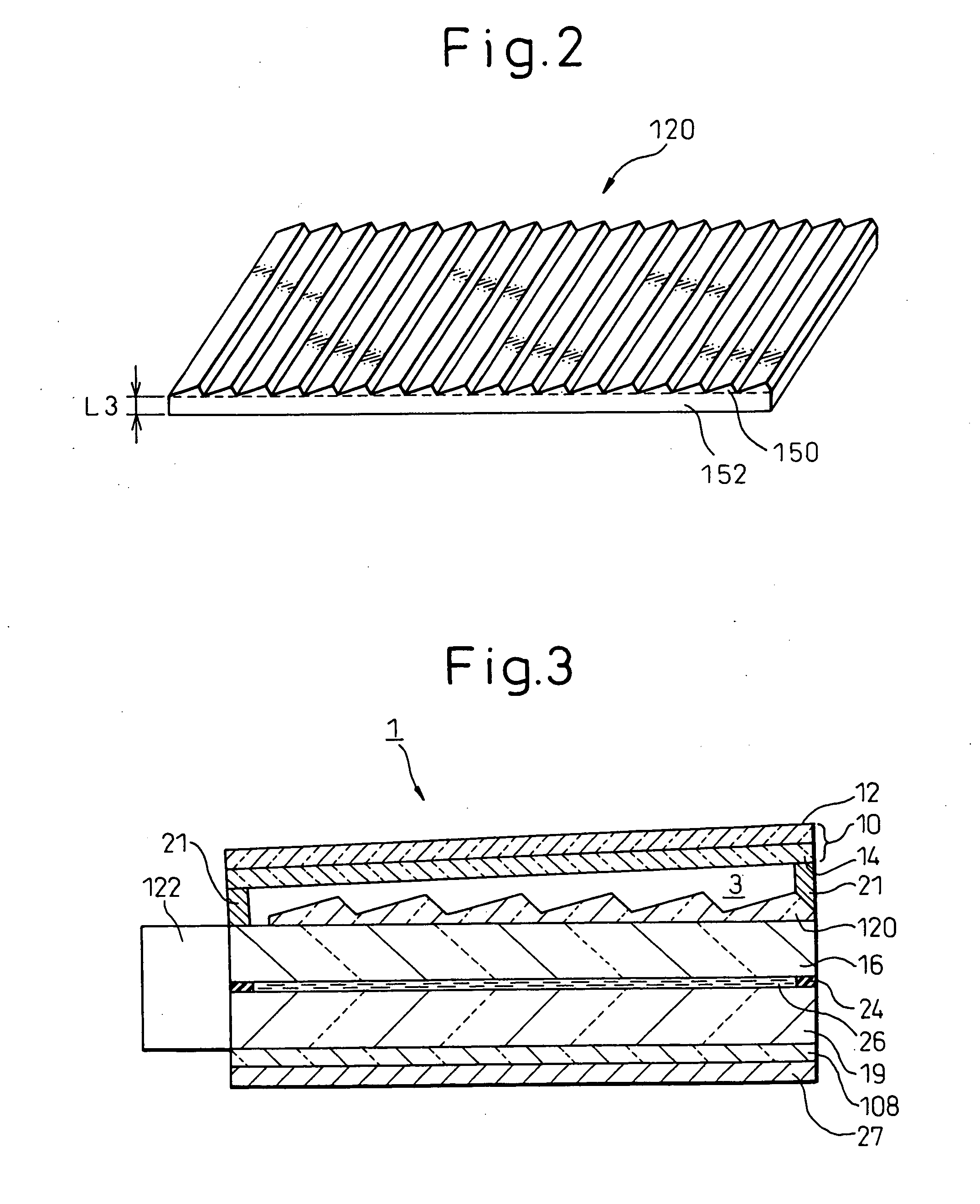
[0130]FIG. 17C shows the structure of a liquid crystal display device 2C in accordance with a third embodiment that is manufactured using a first transparent substrate 16 or a component having a light control member 120 formed thereon according to the manufacturing method shown in FIG. 16A to FIG. 16E, and that includes a reflective layer 27 in a liquid crystal cell thereof. A second transparent substrate 19 is superposed on the side of the first transparent substrate 16 where an electrode (not shown) is provided, with a liquid crystal layer 26 and the reflective layer 27 between them, whereby the liquid crystal cell is produced. The liquid crystal layer 26 is sealed with a sealing member 24 and has a thickness of about 5 μm.

[0131] A difference of the liquid crystal display device 2C from the liquid crystal display device 2A shown in FIG. 17A lies in the disposition of the light control member 120 on the first transparent substrate 16. In the liquid crystal display device 2A in acco...


PUM


Abstract

A liquid crystal is sealed with a sealing member between first and second transparent substrates, whereby a liquid crystal cell capable of transmitting ultraviolet light is produced. The liquid crystal cell is inserted into a mould into which an ultraviolet-setting resin is dropped and which is used to produce a light control member. The ultraviolet-setting resin is pressed to be bonded to the liquid crystal cell. In this state, ultraviolet light is irradiated to the liquid crystal cell in the mould from outside the mould. Thus, the ultraviolet-setting resin is set while bonding to the liquid crystal cell. Thereafter, the liquid crystal cell is removed from the mould. Consequently, the light control member is directly formed on the liquid crystal cell.

Description

CROSS-REFERENCE TO RELATED APPLICATION [0001] This application has priority over, and incorporates by reference, the entire disclosure of Japanese Patent Applications NOS. 2003-173335 and 2003-17336 filed on Jun. 18, 2003. BACKGROUND OF THE INVENTION [0002] 1. Field of the Invention [0003] The present invention relates to a display device and a display device manufacturing method as well as a method of manufacturing the components of the display device. More particularly, the present invention is concerned with a display device including an electro-optic converting member, which can control an amount of transmitted light by utilizing an electric action, such as a liquid crystal cell, and also including a light control member for controlling refraction of light, a method of manufacturing the display device, and a method of manufacturing the components of the display device. [0004] 2. Description of the Related Art [0005] To date, liquid crystal display devices have rapidly been evolv...

Claims


Application Information

Patent Timeline
IPC IPC(8): G02F1/1335
CPCG02F1/133504
Inventor AKIYAMA, TAKASHIMATSUYAMA, KATSUO
Owner CITIZEN WATCH CO LTD
Why Eureka
Try Eureka